Fbar Filter
- Summary
- Abstract
- Description
- Claims
- Application Information
AI Technical Summary
Benefits of technology
Problems solved by technology
Method used
Image
Examples
first embodiment
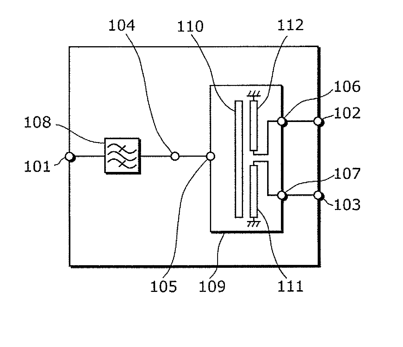
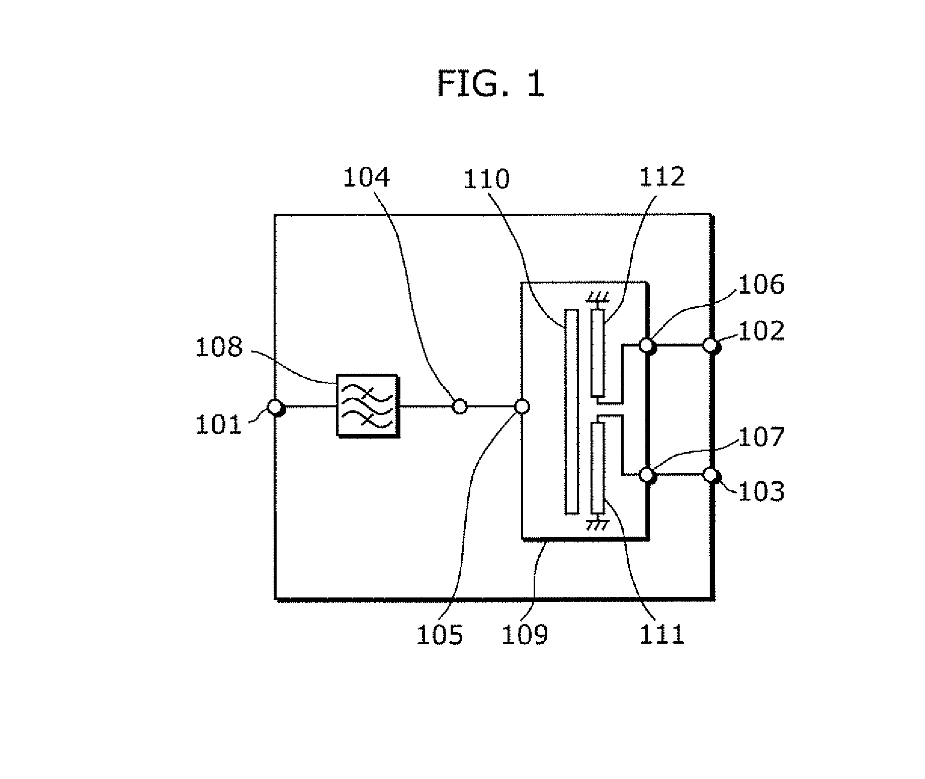
[0107] The FBAR filter according to the first embodiment of the present invention shall be described with reference to FIG. 1. FIG. 1 is a block diagram showing an example of the configuration of the FBAR filter according to the first embodiment of the present invention. The FBAR filter includes an FBAR filter 108 and a balun 109 which are formed on a chip. Here, the balun 109 is used as a balance-unbalance converter
[0108] The FBAR filter 108 has unbalanced input and output terminals 101 and 104. The balun 109 includes an open-end λ / 2 stripline 110 and two shorted-end λ / 4 striplines 111 and 112, and has one input terminal 105 and two output terminals 106 and 107. The unbalanced signal inputted from the input terminal 105 is converted into a balanced signal through the combination of the λ / 2 stripline 110 and the λ / 4 striplines 111 and 112, and outputted from the two output terminals 106 and 107. With this configuration, an FBAR filter having the balance-unbalance conversion functio...
second embodiment
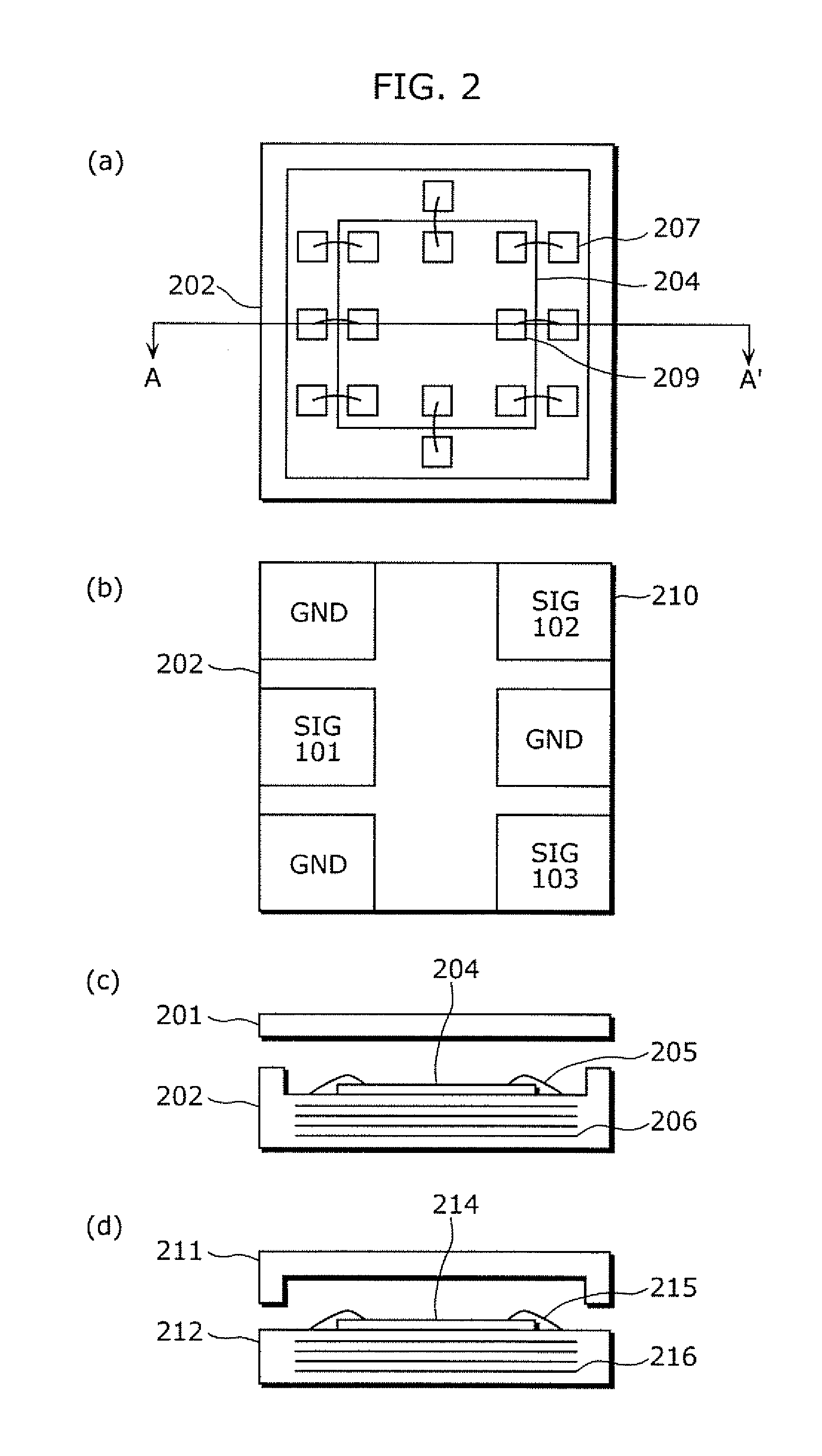
[0110] The FBAR filter according to the second embodiment of the present invention shall be described with reference to FIG. 2. The FBAR filter in this embodiment takes advantage of the previously discussed characteristic of easy formation on a substrate using a semiconductor process. An FBAR filter device prepared as chip is mounted, for example, on a multi-layer substrate and, in addition, sealed in a ceramic package and the like, in order to maintain reliability. Naturally, aside from the ceramic package, sealing with a stainless cap, and the like, is also possible.
[0111]FIG. 2(a) is a top view of the FBAR filter as seen from the cap side (cap is not illustrated). FIG. 2(b) is a bottom view of the FBAR filter. FIG. 2(c) is a A to A′ cross-section of the FBAR filter, and FIG. 2(d) is a cross-section of a variation of the FBAR filter.
[0112] As seen in FIG. 2(c) and (d), the space for storing the FBAR filter chip is created by providing projections on a multi-layer substrate 202 (...
third embodiment
[0120] Next, the FBAR filter according to the third embodiment of the present invention shall be described with reference to FIG. 4. FIG. 4 is a block diagram showing an example of the configuration of the FBAR filter according to the third embodiment of the present invention. The FBAR filter includes a rat race circuit 405 as a balance-unbalance converter.
[0121] An FBAR filter chip 404 has unbalanced input and output terminals. In the rat race circuit 405, as shown in FIG. 4, ports are positioned so that there is a λ / 4 separation between port 406 and port 407, port 407 and port 408, port 408 and port 409, and a 3λ / 4 separation between port 406 and port 409. A signal is inputted from the port 406. In port 407, the signal, which has advanced clockwise for λ / 4 of the ring from port 406, and the signal, which has advanced counter-clockwise for 3λ / 4 of the ring from port 406, are attained. These two signals, which are in-phase, are added together, and outputted from the port 407. Port ...
PUM
 Abstract
Description
Claims
Application Information
 - R&D
- Intellectual Property
- Life Sciences
- Materials
- Tech Scout
- Unparalleled Data Quality
- Higher Quality Content
- 60% Fewer Hallucinations
Browse by: Latest US Patents, China's latest patents, Technical Efficacy Thesaurus, Application Domain, Technology Topic, Popular Technical Reports.
© 2025 PatSnap. All rights reserved.Legal|Privacy policy|Modern Slavery Act Transparency Statement|Sitemap|About US| Contact US: help@patsnap.com


