Display device, and driving method and electronic device thereof
a technology of electronic devices and display devices, applied in static indicating devices, electroluminescent light sources, instruments, etc., can solve the problems of inability to perform sharp display with high contrast, and achieve the effects of high contrast, increased peak luminance in the portion, and sharp image display
- Summary
- Abstract
- Description
- Claims
- Application Information
AI Technical Summary
Benefits of technology
Problems solved by technology
Method used
Image
Examples
embodiment mode 1
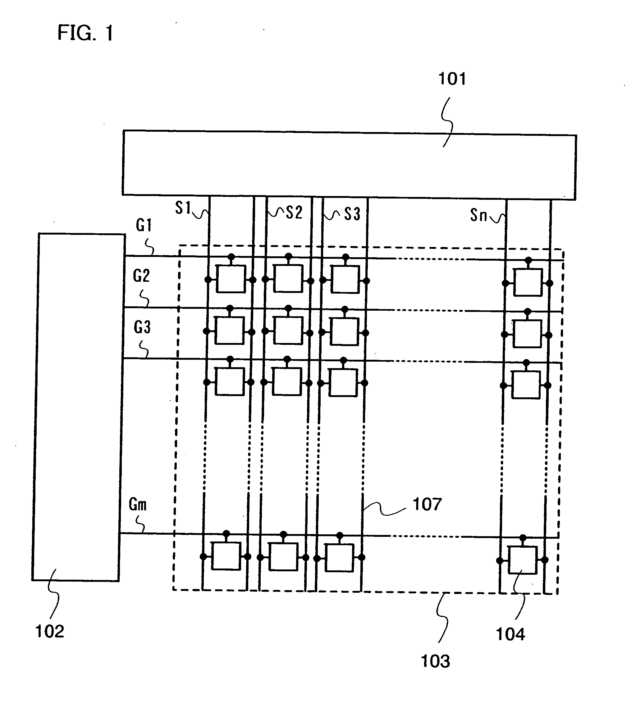
[0094]FIG. 1 shows a basic pixel matrix circuit of a display device of the present invention. This pixel matrix circuit includes a signal line driver circuit 101, a scanning line driver circuit 102, and a pixel portion 103 which is provided with a plurality of pixels 104. In addition, corresponding to scanning lines (G1 to Gm) disposed in rows, signal lines (S1 to Sn) disposed in columns, and power supply lines 107, pixels 104 are disposed in matrix.
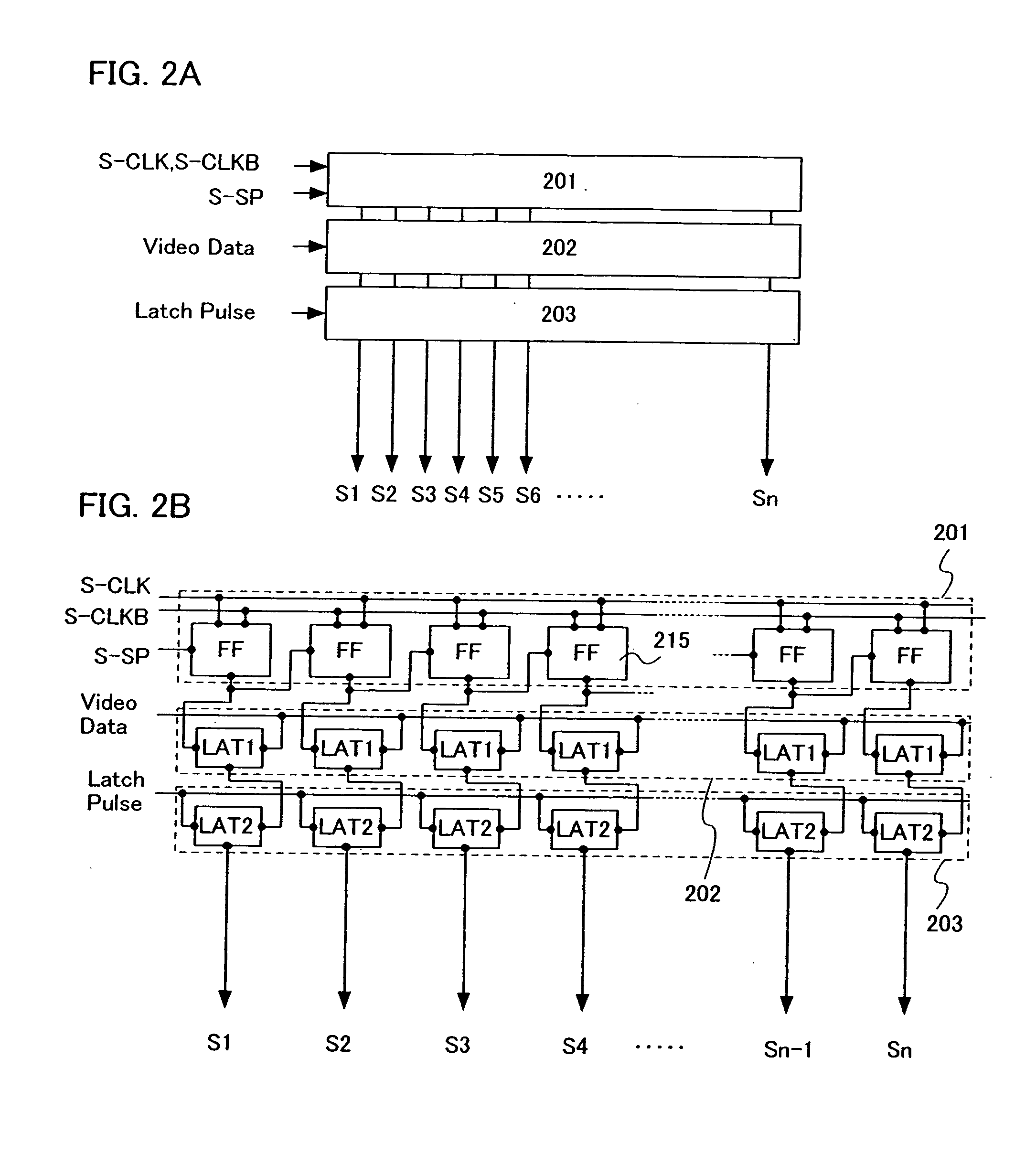
[0095] The signal line driver circuit 101 outputs a video signal to the signal lines S1 to Sn. The scanning line driver circuit 102 outputs a signal for selecting the pixels 104 disposed in rows, to the scanning lines G1 to Gm. Then, the video signal from the signal line driver circuit 101 is written in each pixel 104 of a pixel row selected by the signal that is output from the scanning line driver circuit 102. Note that the signal input to the signal lines S1 to Sn from the signal line driver circuit 101 is not limited to a video sign...
embodiment mode 2
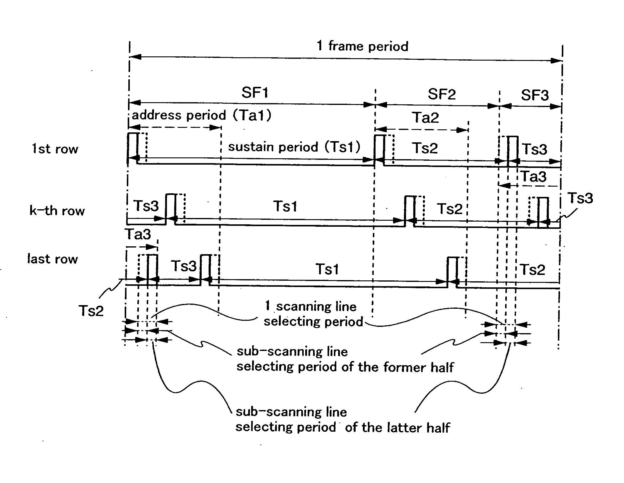
[0144] An operation method of Embodiment Mode 2 will be described with reference to a timing chart of FIG. 8 where a 4-bit gray scale is expressed. The signal writing operation is performed from a first row to an m-th row. Then, a sustain period starts in the row in which the writing operation has been terminated. The next sub-frame starts sequentially in the row in which the sustain period has been terminated, and the signal writing operation is carried out again from the first row. Here, a signal erasing operation is carried out between one signal writing operation and the next signal writing operation, so as to provide a non-lighting period. By providing the signal erasing operation as described above, a sustain period is controlled.
[0145] A circuit configuration of a pixel which is operated in the above-described manner is shown in FIG. 9. A driving TFT 901, a switching TFT 902, a capacitor 903, a light emitting element 904, a first scanning line 905, a signal line 906, a power...
embodiment mode 3
[0158] In Embodiment Mode 3, the case where a signal erasing operation of a pixel is performed with a pixel configuration different from that in Embodiment Mode 2 will be described.
[0159]FIG. 10 shows one example of a pixel configuration in the case the driving TFT is forcibly turned off. A switching TFT 1002, a driving TFT 1001, an erasing diode 1009, and a light emitting element 1004 are provided. One of a source region and a drain region of the switching TFT 1002 is connected to a signal line 1006, and the other is connected to a gate electrode of the driving TFT 1001, the capacitor 1003, and the erasing diode 1009. A gate electrode of the switching TFT 1002 is connected to a first scanning line 1005. One of a source region and a drain region of the driving TFT 1001 is connected to a power supply line 1007, and the other is connected to the light emitting element 1004. An input terminal of the erasing diode 1009 is connected to a second scanning line 1010, and an output terminal...
PUM
 Abstract
Description
Claims
Application Information
 - R&D
- Intellectual Property
- Life Sciences
- Materials
- Tech Scout
- Unparalleled Data Quality
- Higher Quality Content
- 60% Fewer Hallucinations
Browse by: Latest US Patents, China's latest patents, Technical Efficacy Thesaurus, Application Domain, Technology Topic, Popular Technical Reports.
© 2025 PatSnap. All rights reserved.Legal|Privacy policy|Modern Slavery Act Transparency Statement|Sitemap|About US| Contact US: help@patsnap.com


