Analog-to-digital conversion circuit

a conversion circuit and analog-to-digital technology, applied in analogue/digital conversion, transmission systems, instruments, etc., can solve the problems of increasing the range of applications of parallel-type analog-to-digital conversion systems, increasing power consumption and chip size correspondingly, and reducing the range of offset variations. , the effect of reducing power consumption

Inactive Publication Date: 2007-08-16
SONY CORP
View PDF7 Cites 9 Cited by
  • Summary
  • Abstract
  • Description
  • Claims
  • Application Information

AI Technical Summary

Benefits of technology

[0014] According to another embodiment of the present invention, the output terminals are connected to each other by the averaging resistive elements in each of the stages of the first amplifying unit and the second amplifying unit, and further the averaging process by majority logic operation is performed in a binary signal stage. It is thereby possible to reduce offset variations even when the size of circuit elements is relatively small, and thus achieve a smaller area and lower power consumption.

Problems solved by technology

Therefore, when the resolution is to be raised, circuit scale is increased exponentially, and power consumption and chip size are correspondingly increased.
Thus a range of applications of the parallel type analog-to-digital conversion system tends to be limited.

Method used


Image

  • Analog-to-digital conversion circuit
  • Analog-to-digital conversion circuit
  • Analog-to-digital conversion circuit

Examples


first embodiment

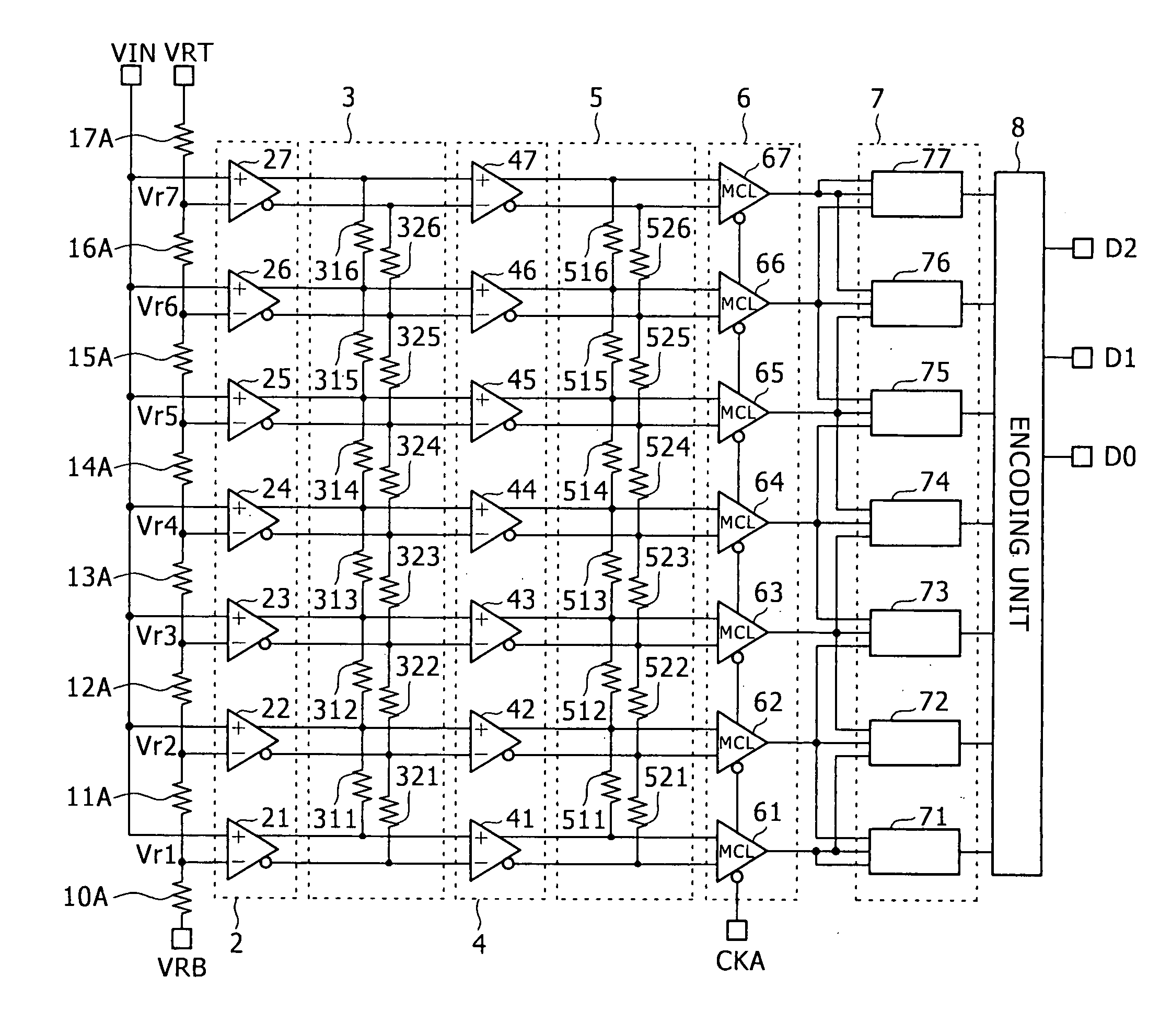
[0029]FIG. 1 is a diagram showing an example of configuration of a three-bit analog-to-digital conversion circuit according to a first embodiment of the present invention.

[0030] The analog-to-digital conversion circuit shown in FIG. 1 includes resistive elements 10A to 17A for generating reference voltages, a first amplifying unit 2, a first averaging unit 3, a second amplifying unit 4, a second averaging unit 5, a comparing unit 6, a third averaging unit 7, and an encoding unit 8.

[0031] The first amplifying unit 2 is an embodiment of a first amplifying unit according to the present invention.

[0032] The second amplifying unit 4 is an embodiment of a second amplifying unit according to the present invention.

[0033] The first averaging unit 3 is an embodiment of a first averaging unit according to the present invention.

[0034] The second averaging unit 5 is an embodiment of a second averaging unit according to the present invention.

[0035] The comparing unit 6 is an embodiment of a...

second embodiment

[0097] A second embodiment of the present invention will next be described.

[0098] An analog-to-digital conversion circuit according to the second embodiment is provided with a folder circuit and an interpolating circuit.

[0099]FIG. 6 is a diagram showing an example of configuration of the three-bit analog-to-digital conversion circuit according to the second embodiment of the present invention.

[0100] The analog-to-digital conversion circuit shown in FIG. 6 has resistive elements 10A to 15A for generating reference voltages, a first amplifying unit 2A, a first averaging unit 3A, a folder circuit 9, a coarse amplifier 10, an interpolating circuit 11, a second averaging unit 5A, a comparing unit 6A, a third averaging unit 7A, and an encoding unit 8.

[0101] The first amplifying unit 2A is an embodiment of a first amplifying unit according to the present invention.

[0102] The folder circuit 9 is an embodiment of a folder circuit according to the present invention.

[0103] The coarse amp...


PUM


Abstract

Disclosed herein is an analog-to-digital conversion circuit configured to convert an input analog signal into a digital signal, said analog-to-digital conversion circuit includes: a first amplifying unit; a second amplifying unit; a comparing unit; a first averaging unit; a second averaging unit; and a third averaging unit.

Description

CROSS REFERENCES TO RELATED APPLICATIONS [0001] The present invention contains subject matter related to Japanese Patent Application JP 2006-006134 filed in the Japanese Patent Office on Jan. 13, 2006, the entire contents of which being incorporated herein by reference. BACKGROUND OF THE INVENTION [0002] 1. Field of the Invention [0003] The present invention relates to an analog-to-digital conversion circuit configured to convert an input analog signal into a digital signal, and particularly to a parallel type analog-to-digital conversion circuit that achieves a smaller area and lower power consumption. [0004] 2. Description of the Related Art [0005]FIG. 13 is a diagram showing an example of configuration of an ordinary parallel type analog-to-digital conversion circuit. [0006] The analog-to-digital conversion circuit shown in FIG. 13 has a resistance ladder (R1 to R8) for generating a plurality of reference voltages, amplifier circuits A1 and A2 in two stages, master comparator lat...

Claims


Application Information

Patent Timeline
Patent Type & Authority Applications(United States)
IPC IPC(8): H03M1/12
CPCH03M1/365H03M1/0646H03M1/36
Inventor MAKIGAWA, KIYOSHIONO, KOICHIOHKAWA, TAKESHI
Owner SONY CORP
Why Eureka
Try Eureka