Plasma display panel and method for manufacturing the same

a technology of display panel and plasma, which is applied in the manufacture of tube/lamp screen, gas-filled discharge tube, incadescent envelope/vessel, etc., can solve the problems of reducing yield rate and difficult manufacturing process, and achieve the effect of improving contrast and color performance of pdp, increasing secondary electrons, and improving the quality of pdp

Inactive Publication Date: 2007-08-02
MARKETECH INT
View PDF2 Cites 4 Cited by
  • Summary
  • Abstract
  • Description
  • Claims
  • Application Information

AI Technical Summary

Benefits of technology

[0010]In this embodiment, the glass substrate has a first surface and a second surface opposite to the first surface. The transparent conductive layer is formed on the first surface of the glass substrate. The bus electrodes are formed on the second surface of the glass substrate and used for providing a current. The dielectric layer is formed on the second surface of the glass substrate and covers the bus electrodes. The dielectric layer is used for restraining the current, so as to accumulating wall charge. The first protective layer is formed on the dielectric layer and used for preventing the front panel from being attacked by ions and increasing secondary electrons. The second protective layer is formed on the transparent conductive layer and used for improving contrast and color performance of the PDP and protecting the front panel from damage. The back panel is attached to the first protective layer of the front panel to complete the PDP.
[0011]According to the aforementioned embodiment, an area of the second protective layer is smaller than that of the transparent conductive layer, such that the exposed transparent conductive layer is capable of being grounded to the inner component of the PDP, so as to shield off EMI.
[0012]Therefore, since parts of the transparent conductive layer are exposed out of the second protective layer, the exposed transparent conductive layer is capable of being grounded to the inner component of the PDP, so as to shield off EMI. In other words, there is no additional metal structure in the second protective layer, such that the second protective layer can be easily attached onto the transparent conductive layer. Therefore, the manufacturing of PDP is getting much easier, and the yield rate will then increase.
[0013]The advantage and spirit of the invention may be understood by the following recitations together with the appended drawings.

Problems solved by technology

Consequently, it will be difficult to attach the filter glass 110 or the filter film to the glass substrate 108 of the front panel due to the metal structure, so that the manufacturing process is getting much more difficult, and then the yield rate will decrease.

Method used


Image

  • Plasma display panel and method for manufacturing the same
  • Plasma display panel and method for manufacturing the same
  • Plasma display panel and method for manufacturing the same

Examples


Embodiment Construction

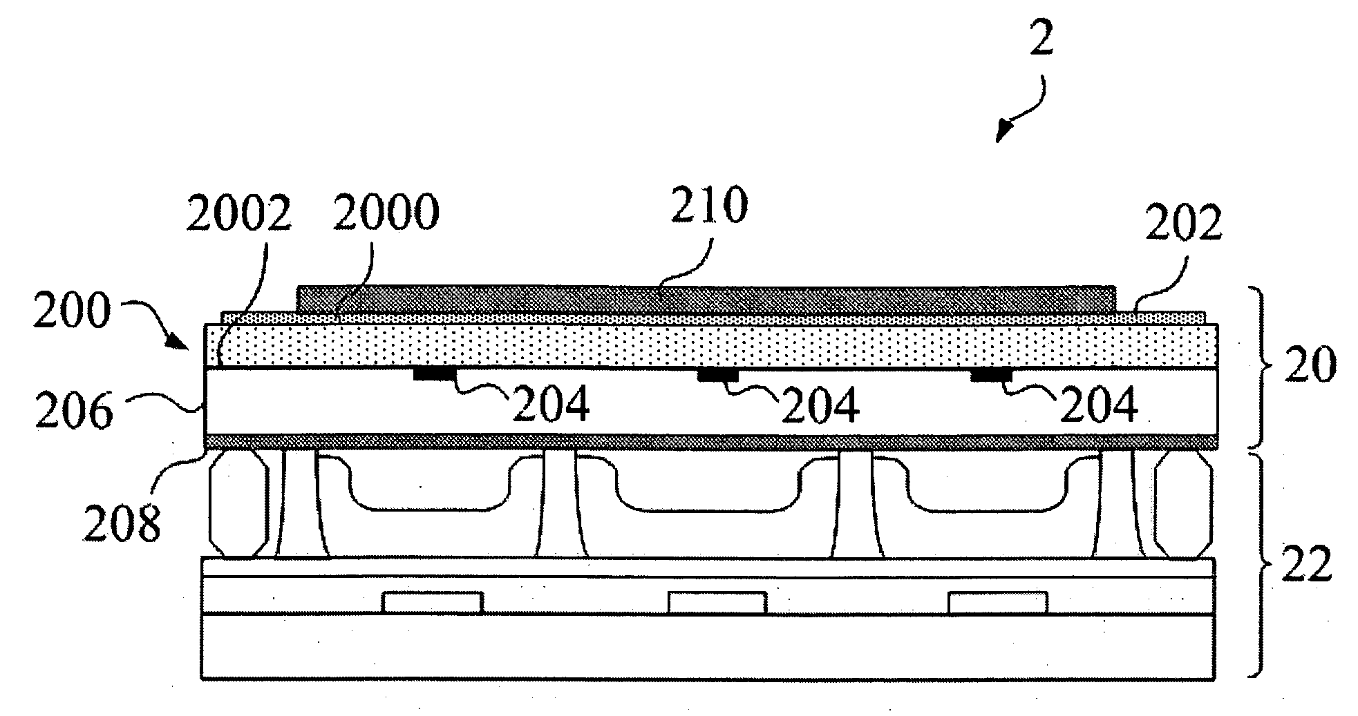
[0019]Referring to FIG. 3A, FIG. 3A is a schematic diagram illustrating the PDP 2 according to a preferred embodiment of the invention. The PDP 2 includes a front panel 20 and a back panel 22. The front panel 20 includes a glass substrate 200, a transparent conductive layer 202, at least one bus electrodes 204, a dielectric layer 206, a first protective layer 208 and a second protective layer 210. In this embodiment, the transparent conductive layer can be made of ITO, SnO2 or the like, the first protective layer can be made of MgO or the like, and the second protective layer can be a thick film.

[0020]As shown in FIG. 3A, the glass substrate 200 has a first surface 2000 and a second surface 2002 opposite to the first surface 2000. The transparent conductive layer 202 is formed on the first surface 2000 of the glass substrate 200. The bus electrodes 204 are formed on the second surface 2002 of the glass substrate 200 and used for providing a current. The dielectric layer 206 is forme...


PUM


Abstract

The invention discloses a plasma display panel (PDP). The PDP grounds an exposed transparent conductive layer to the inner component thereof, so as to shield off electromagnetic interference (EMI). Accordingly, there is no metal structure in the second protective layer formed on the transparent conductive layer, such that the second protective layer can be easily attached onto the transparent conductive layer. Therefore, the manufacturing of PDP is getting much easier, and the yield rate will then increase.

Description

BACKGROUND OF THE INVENTION[0001]1. Field of the Invention[0002]The invention relates to a plasma display panel (PDP) and method for manufacturing the same.[0003]2. Description of the Prior Art[0004]Referring to FIG. 1, FIG. 1 is a schematic diagram illustrating the conventional PDP 1. As shown in FIG. 1, the conventional PDP 1 includes a front panel 10 and a back panel 12. The front panel 10 includes a protective layer 100 such as MgO, a dielectric layer 102, at least one bus electrode 104, a transparent conductive layer 106 such as ITO, a glass substrate 108 and a filter glass 110. The filter glass 110 is used for improving contrast and color performance of the PDP 1. Furthermore, the filter glass 110 has a metal structure therein capable of shielding off electromagnetic interference (EMI).[0005]Referring to FIGS. 2A through 2D, FIGS. 2A through 2D respectively illustrate the process of manufacturing the PDP 1 shown in FIG. 1. As shown in FIG. 2A, at start, the glass substrate 108...

Claims


Application Information

Patent Timeline
Patent Type & Authority Applications(United States)
IPC IPC(8): H01J61/40H01J17/49
CPCH01J9/205H01J11/12H01J2211/446H01J11/44H01J2211/444H01J11/40
Inventor KAO, HSU-PINLIANG, JANG-JENGHSU, SHENG-WENKAO, HSU-CHIAYU, YI-SHENG
Owner MARKETECH INT
Why Eureka
Try Eureka