
Electroluminescence panel and method of making the same

a technology of electroluminescence panel and el panel, which is applied in the direction of discharge tube luminescnet screen, discharge tube/lamp details, electric discharge lamps, etc., can solve the problems of reducing the emission area, reducing the luminance of the device, and damaging the el device, so as to reduce the emission area and reduce the amount of resin components

Inactive Publication Date: 2007-07-12
FUTABA CORPORATION
View PDF6 Cites 0 Cited by
  • Summary
  • Abstract
  • Description
  • Claims
  • Application Information

AI Technical Summary

Benefits of technology

[0008] For solving the problem mentioned above, it is an object of the present invention to provide an EL panel which can restrain a sealing resin from deteriorating characteristics of EL devices even when sealed with a resin, and a method of making the same.
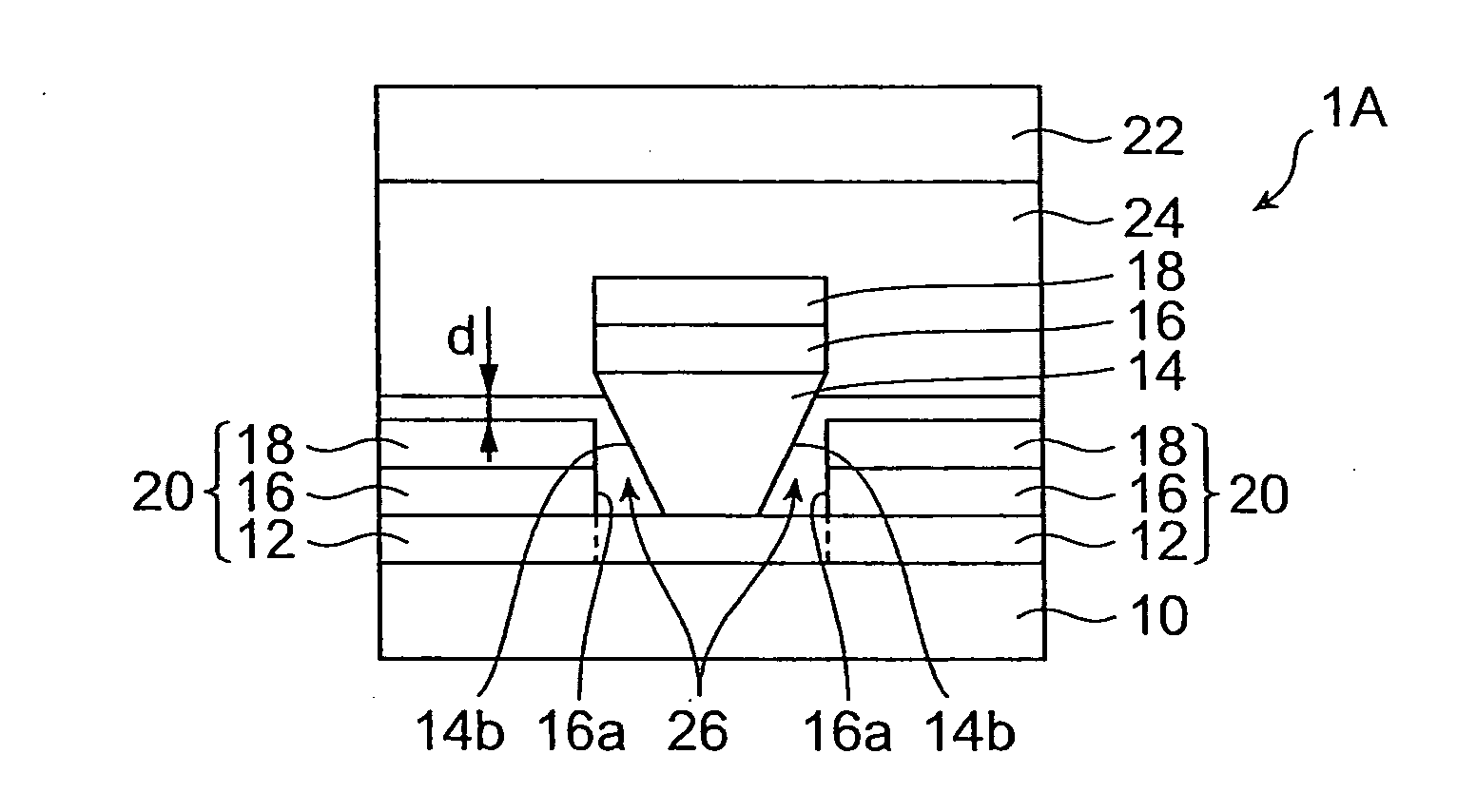
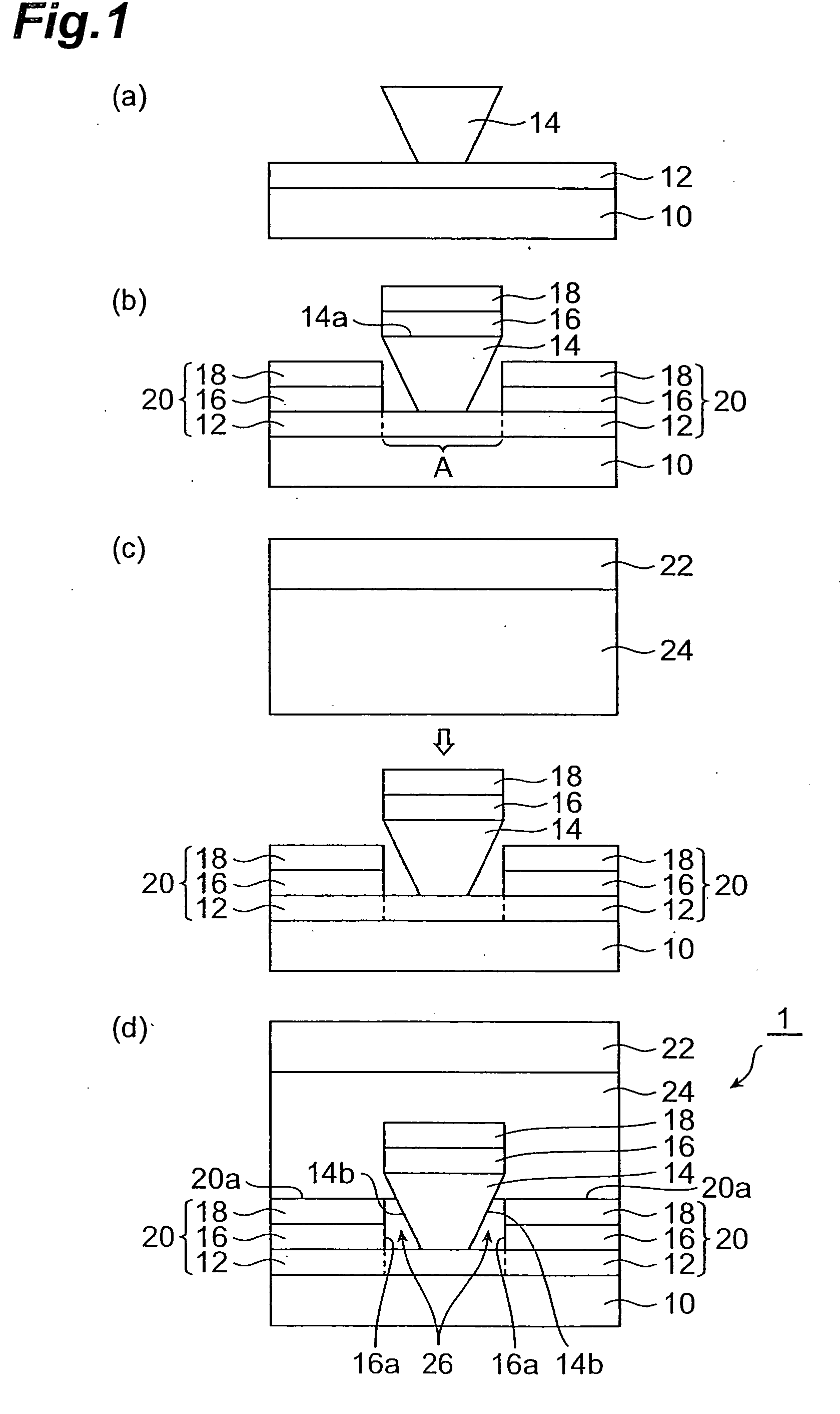
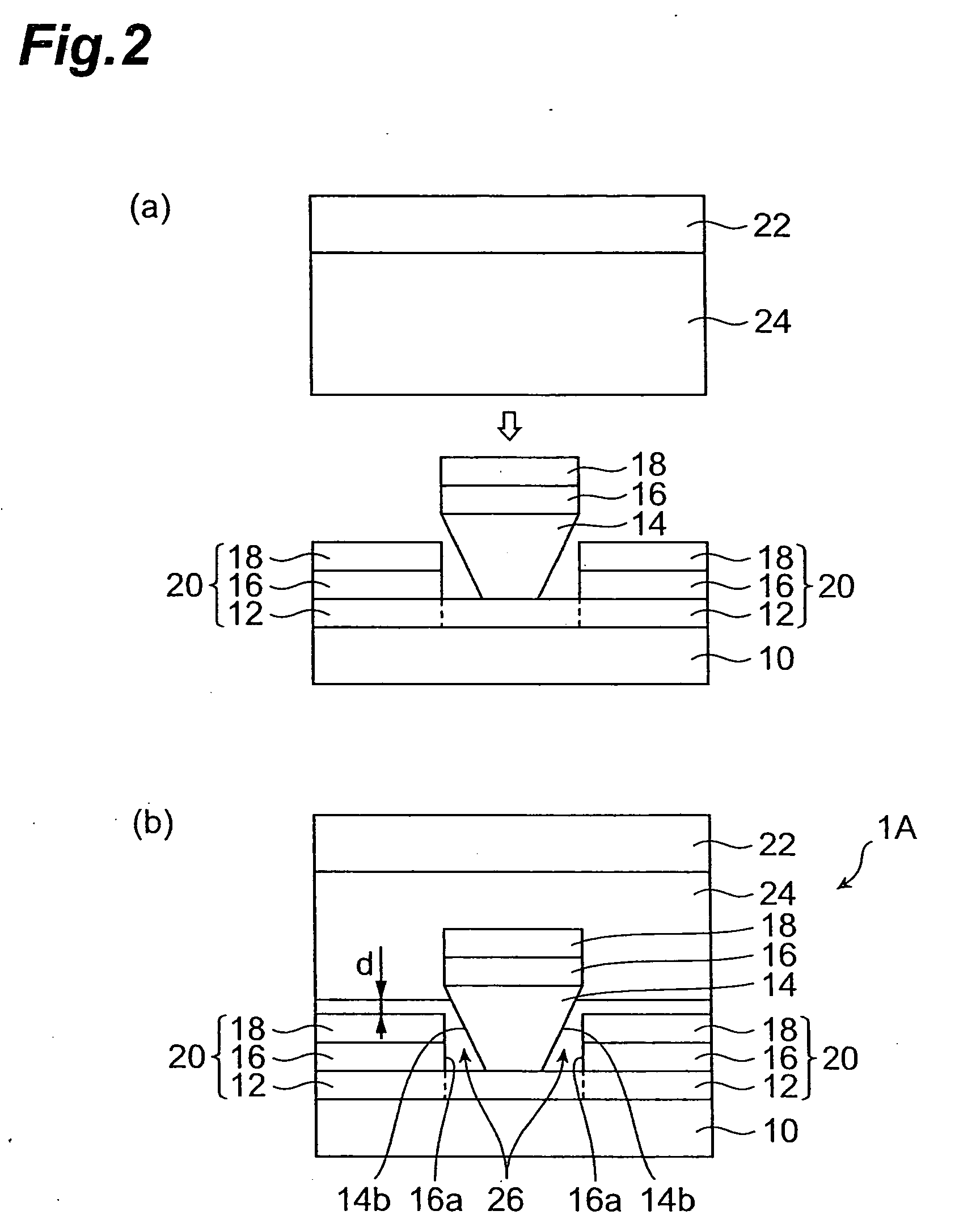
[0010] Since a space is formed between the wall and the organic layer of the EL devices in this EL panel, the gap between the substrate and the sealing plate is sealed with the resin while the sealing resin is not in contact with the end face of the organic layer on the wall side. This significantly restrains resin components in the sealing resin from eroding the organic layer of the EL devices. Therefore, the sealing resin is kept from deteriorating characteristics of the EL devices in the EL panel in accordance with the present invention.
[0011] Preferably, the wall and the resin are in contact with each other. In this case, the void between the adjacent walls is clogged with the resin, which suppresses the flow of air traveling by way of the walls, whereby the EL devices are kept from being influenced by the air.
[0012] Preferably, the space is a vacuum or filled with an inert gas. In this case, no air exists in the space, whereby the EL devices are more effectively kept from deteriorating their characteristics.
[0014] In this method of making an EL panel, a space is formed between the wall and the organic layer of the EL devices when bonding the sealing plate and the substrate to each other. That is, the gap between the substrate and the sealing plate is sealed with the resin while the sealing resin is not in contact with the end face of the organic layer on the wall side. This significantly restrains resin components of the sealing resin from eroding the organic layer of the EL devices. Therefore, the method of making an EL panel in accordance with the present invention yields an EL panel in which the sealing resin is kept from deteriorating characteristics of the EL devices.
[0015] A sealing plate coated with a resin in an uncured state may cover a plurality of EL devices and the wall. In this case, the upper part of the wall is buried in the resin, which can fully prevent water from entering from the external environment.

Problems solved by technology

Making an EL panel by bringing a resin and an EL device into contact with each other may damage the EL device.
When the EL device is thus damaged, the original emission of the EL device may not be obtained sufficiently, whereby the EL device may lower its luminance and decrease its emission area.

Method used


Image

  • Electroluminescence panel and method of making the same
  • Electroluminescence panel and method of making the same
  • Electroluminescence panel and method of making the same

Examples


examples

[0039] Details of the present invention will now be explained with reference to examples.

example

[0040] Using the manufacturing method shown in the above-mentioned embodiment, the inventors made an EL panel #1 similar to the EL panel 1 by the following procedure.

[0041] First, a plurality of anodes made of ITO (tin-doped indium oxide) were formed by patterning on a transparent substrate (glass substrate). Thereafter, a plurality of walls (walls made of a positive photosensitive resist (based on a novolac resin)) were formed in the aligning direction of the anodes 12 (see part (a) of FIG. 1).

[0042] Next, an organic layer (formed by laminating 4,4′, 4″-tris(3-methylphenylphenylamino)phenylamine (MTDATA), N,N,N′,N′-tetrakis(3-biphenyl)-4,4′-diamino-1,1′-biphenyl (TPD), and Alq3:tris(8-quinolinato)aluminum in this order) and a cathode (formed by laminating an Ag / Mg alloy and Al in this order) were successively laminated by vapor deposition on the whole surface of the region formed with the anodes and walls in the transparent substrate surface (see part (b) of FIG. 1). Here, the an...


PUM


Abstract

An EL panel which can restrain a sealing resin from deteriorating characteristics of EL devices even when sealed with the resin, and a method of making the same are provided. An EL panel 1 in accordance with the present invention comprises a plurality of EL devices 20 constructed by successively laminating an anode 12, an organic layer 16, and a cathode 18 on a transparent substrate 10; walls 14 positioned between the EL devices 20 adjacent to each other; and a sealing plate 22 integrally covering the plurality of EL devices 20 and walls 14; wherein a resin 24 is interposed between the transparent substrate 10 and the sealing plate 22, while a space 26 is formed between the wall 14 and the organic layer 16 of the EL devices 20, whereby resin components of the sealing resin 24 are significantly restrained from eroding the organic layer 16 of the EL devices 20.

Description

BACKGROUND OF THE INVENTION [0001] 1. Field of the Invention [0002] The present invention relates to an EL panel and a method of making the same. [0003] 2. Related Background Art [0004] EL (Electro Luminescence) devices such as organic and inorganic EL devices are light-emitting devices of self-emission type characterized in that they are easy to reduce their size and weight while exhibiting a high luminance, and thus are expected to be employed in displays, illuminations, and the like. However, luminous materials used in these EL devices tend to be easily deteriorated by air (its water content such as moisture in particular), which is one of factors preventing the devices from achieving a longer life. Therefore, the EL devices have conventionally been in use in the form of EL panels sealing the devices therein in order to make them less likely to come into contact with air. [0005] Known as a mode of such sealing is that of hollow type in which an EL device is arranged between a sub...

Claims


Application Information

Patent Timeline
Patent Type & Authority Applications(United States)
IPC IPC(8): H05B33/04
CPCH01L51/5237H01L27/3295H10K59/173H10K50/8426H05B33/04H05B33/22
Inventor SATOMI, NORIAKIAZUMA, YUKIHIRO
Owner FUTABA CORPORATION
Learn More