Method of manufacturing semiconductor device

Inactive Publication Date: 2007-06-14
DONGBU HITEK CO LTD
View PDF7 Cites 2 Cited by
  • Summary
  • Abstract
  • Description
  • Claims
  • Application Information

AI Technical Summary

Benefits of technology

[0007] Consistent with the present invention, there is provided a manufacturing method of a semiconductor device having a short-channel transistor su

Problems solved by technology

However, a short-channel effect which reduces the effective channel length occurs due to the lateral diffusion of source / drain diffusion layer.
However, the reduction of the amount of ion implantation in a lightly doped junction region gives rise to problems such as deterioration caused by a hot carrier effect becomes more noticeable and the resistance of the lightly doped junction region is increased.
Moreover, the formation of salicide is disturbed by the narrow line effect, thereby leading to an increase in the resistance of a gate electrode.
This causes a transistor operating signal of a semiconductor device to be distorted, which lowers the reliability of the semiconductor device.

Method used


Image

  • Method of manufacturing semiconductor device
  • Method of manufacturing semiconductor device
  • Method of manufacturing semiconductor device

Examples


Embodiment Construction

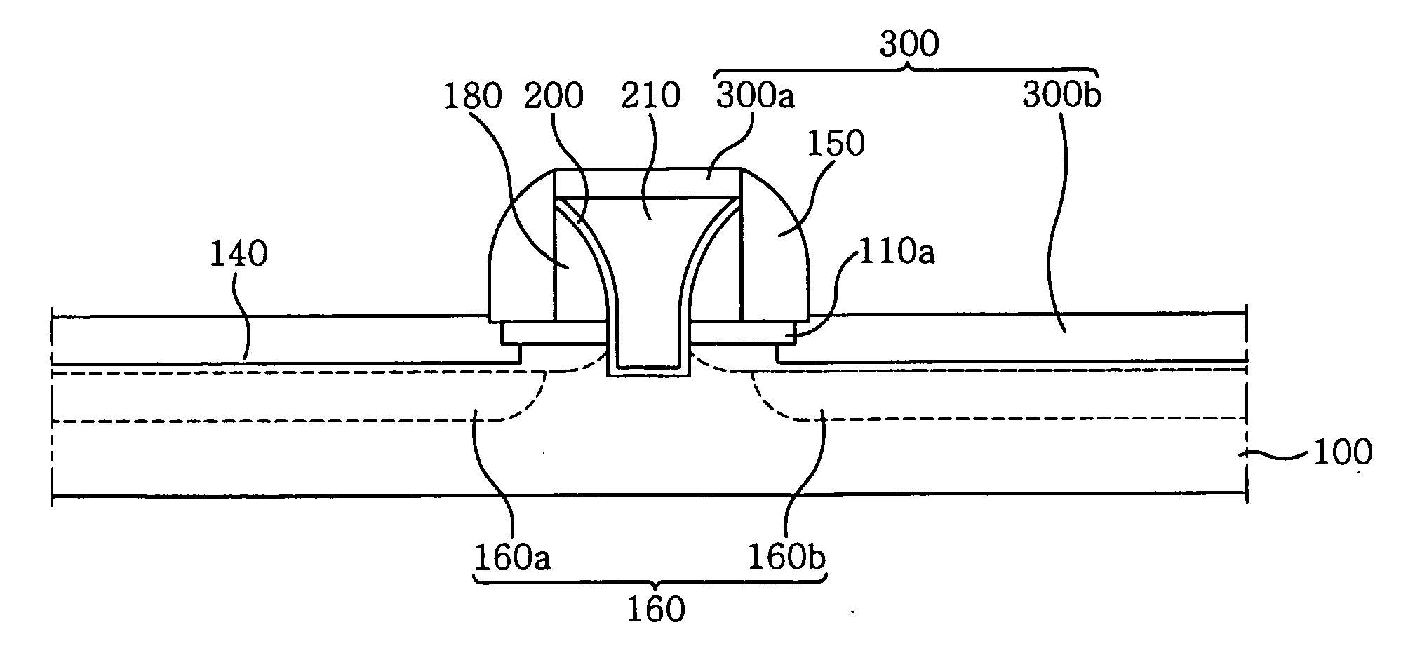
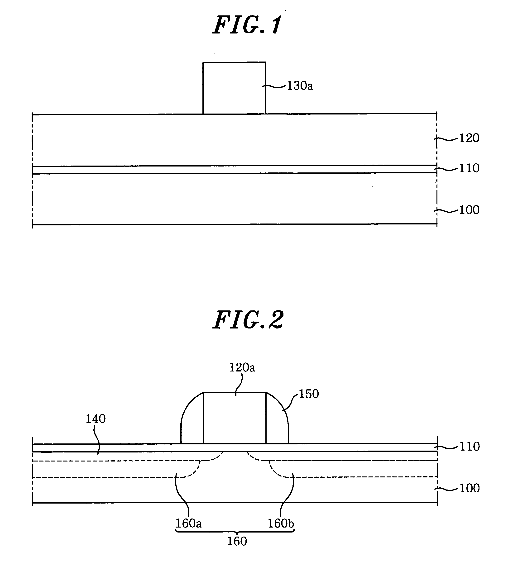
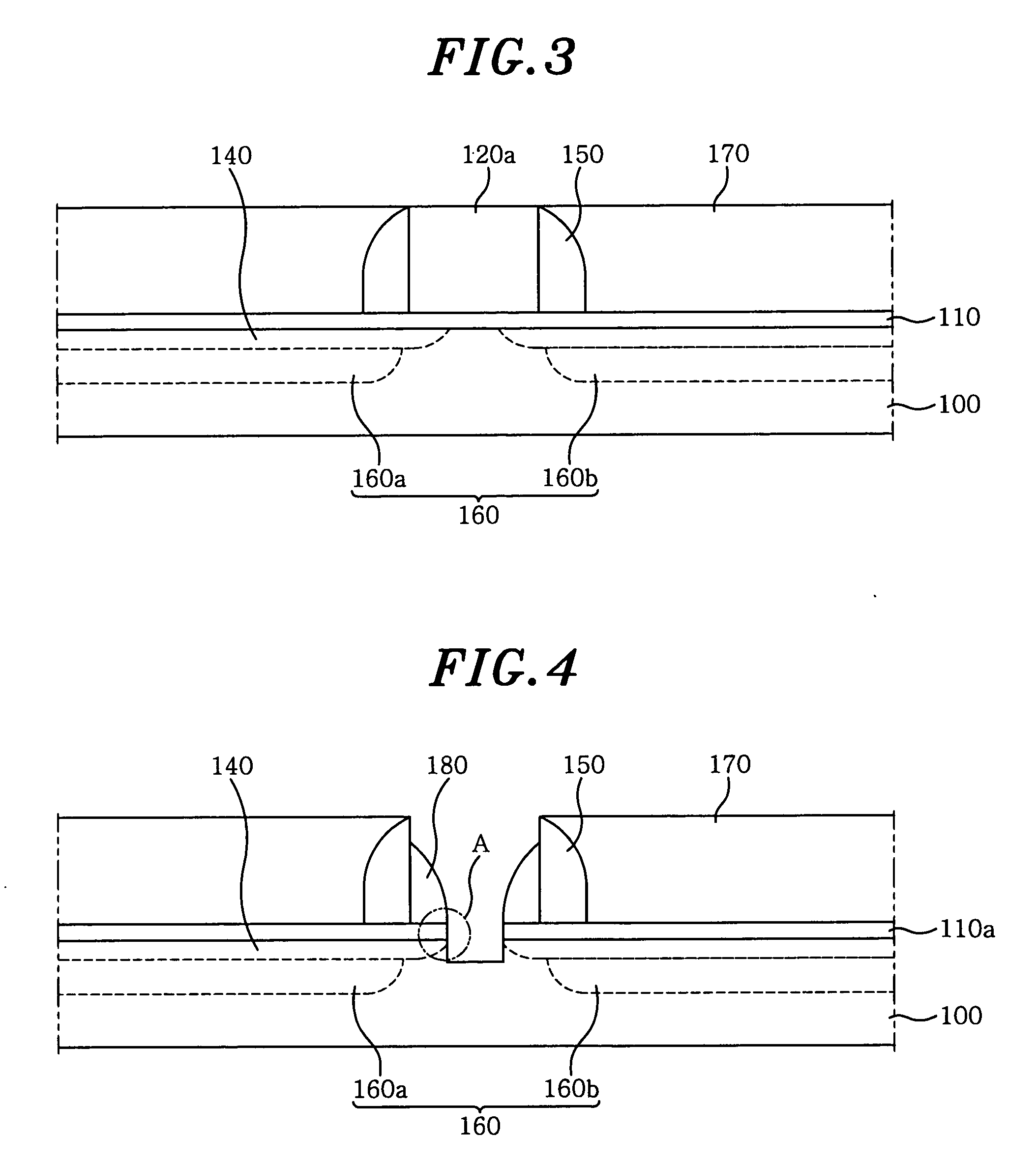
[0012] Hereinafter, an embodiment of the present invention will be described in detail with reference to the accompanying drawings so that the invention can readily be carried out by those skilled in the art to which the invention pertains. However, the present invention may be implemented in many different forms, and therefore, is not limited to the embodiment illustrated herein.

[0013] In the drawings, the thickness of layers, films, panels, regions, etc., are exaggerated for clarity. Like reference numerals designate like elements throughout the specification. It will be understood that when an element such as a layer, film, region, or substrate is referred to as being “on” another element, it may be directly on the other element or intervening elements may also be present. In contrast, when an element is referred to as being “directly on” another element, no intervening elements are present.

[0014] FIGS. 1 to 7 are cross-sectional views sequentially showing respective steps of a...


PUM


Abstract

A method for manufacturing a semiconductor device, includes sequentially forming a first insulation film and a dummy gate electrode on a semiconductor substrate; forming a lightly doped junction region by using the dummy gate electrode as a mask, forming a first spacer on a side wall of the dummy gate electrode, and then forming a heavily doped junction region. The method further includes forming a second insulation film on the semiconductor substrate where the heavily doped junction region is formed, and removing the dummy gate electrode to form a cavity exposing a portion of the first insulation layer; forming a second spacer on a side wall of the cavity; sequentially forming a gate insulation film and a gate conductor on the second spacer, and then removing the second insulation film and a portion of the gate insulation film; and forming a salicide film on a top of the gate conductor and in the lightly doped junction region.

Description

RELATED APPLICATION [0001] This application is based upon and claims the benefit of priority to Korean Application No. 10-2005-0123282, filed on Dec. 14, 2005, the entire contents of which are incorporated herein by reference. TECHNICAL FIELD [0002] The present invention relates to a manufacturing method of a semiconductor device. BACKGROUND [0003] As semiconductor devices are gradually becoming more highly-integrated, a short-channel transistor fabrication technology is required. However, a short-channel effect which reduces the effective channel length occurs due to the lateral diffusion of source / drain diffusion layer. In general, the short-channel effect reduces the amount of ion implantation in a lightly doped junction region, thus minimizing the effect thereof. [0004] In addition, as the length of a gate electrode is shortened, a narrow line effect occurs. Since the narrow line effect disturbs the formation of salicide, the effect of disturbance is minimized in such a manner t...

Claims


Application Information

Patent Timeline
IPC IPC(8): H01L21/336H01L29/76
CPCH01L29/42376H01L29/665H01L29/66545H01L29/66553H01L29/66621H01L29/7833H01L21/24
Inventor PARK, JEONG-HO
Owner DONGBU HITEK CO LTD
Why Eureka
Try Eureka