
Integrated etched multilayer grating based wavelength demultiplexer

Inactive Publication Date: 2007-04-19
MCGILL UNIV
View PDF13 Cites 69 Cited by
  • Summary
  • Abstract
  • Description
  • Claims
  • Application Information

AI Technical Summary

Problems solved by technology

Such roadmaps very quickly limit even the capacity of today's largest 80 channel 10 Gb / s communications backbone networks.
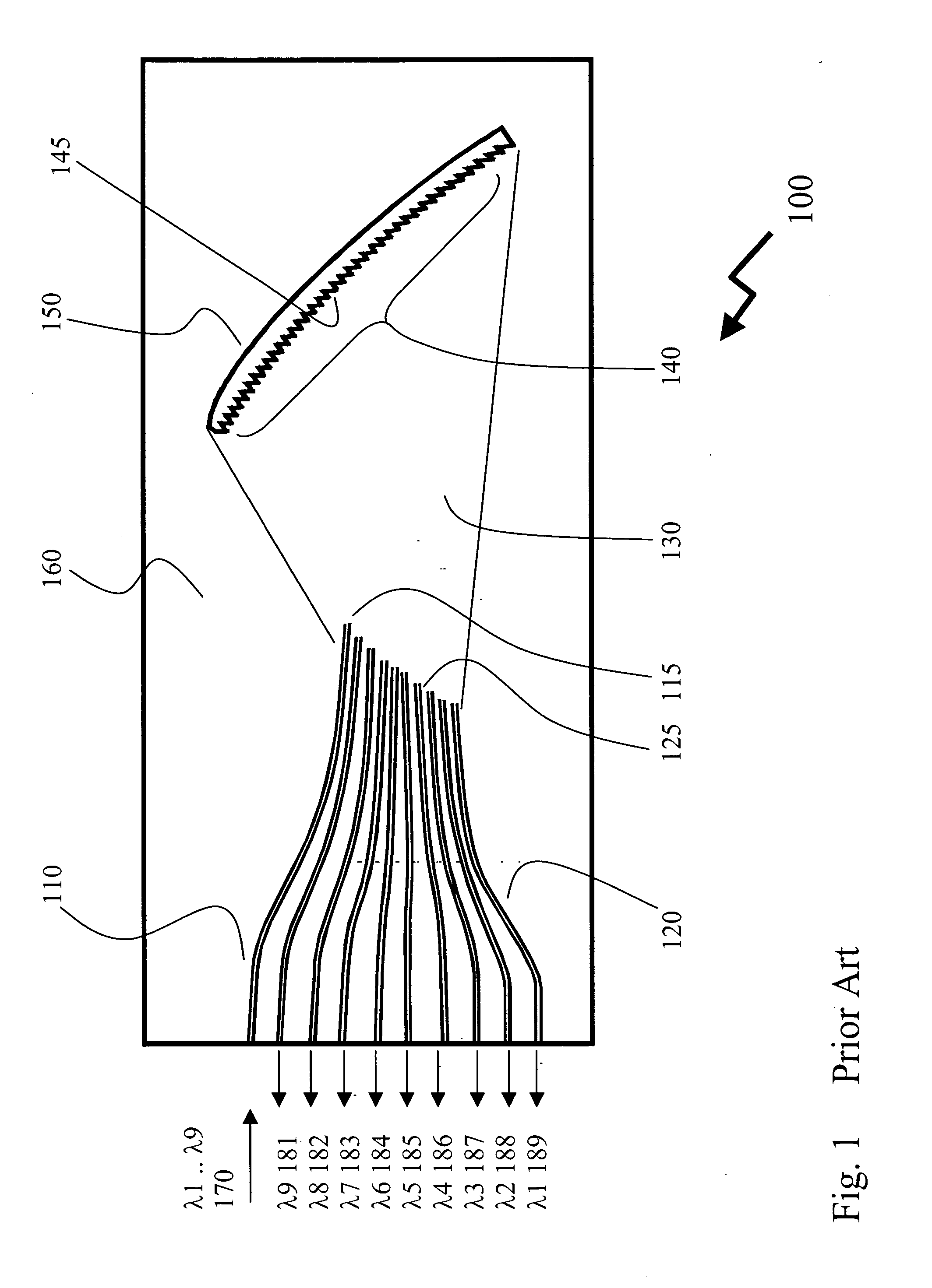
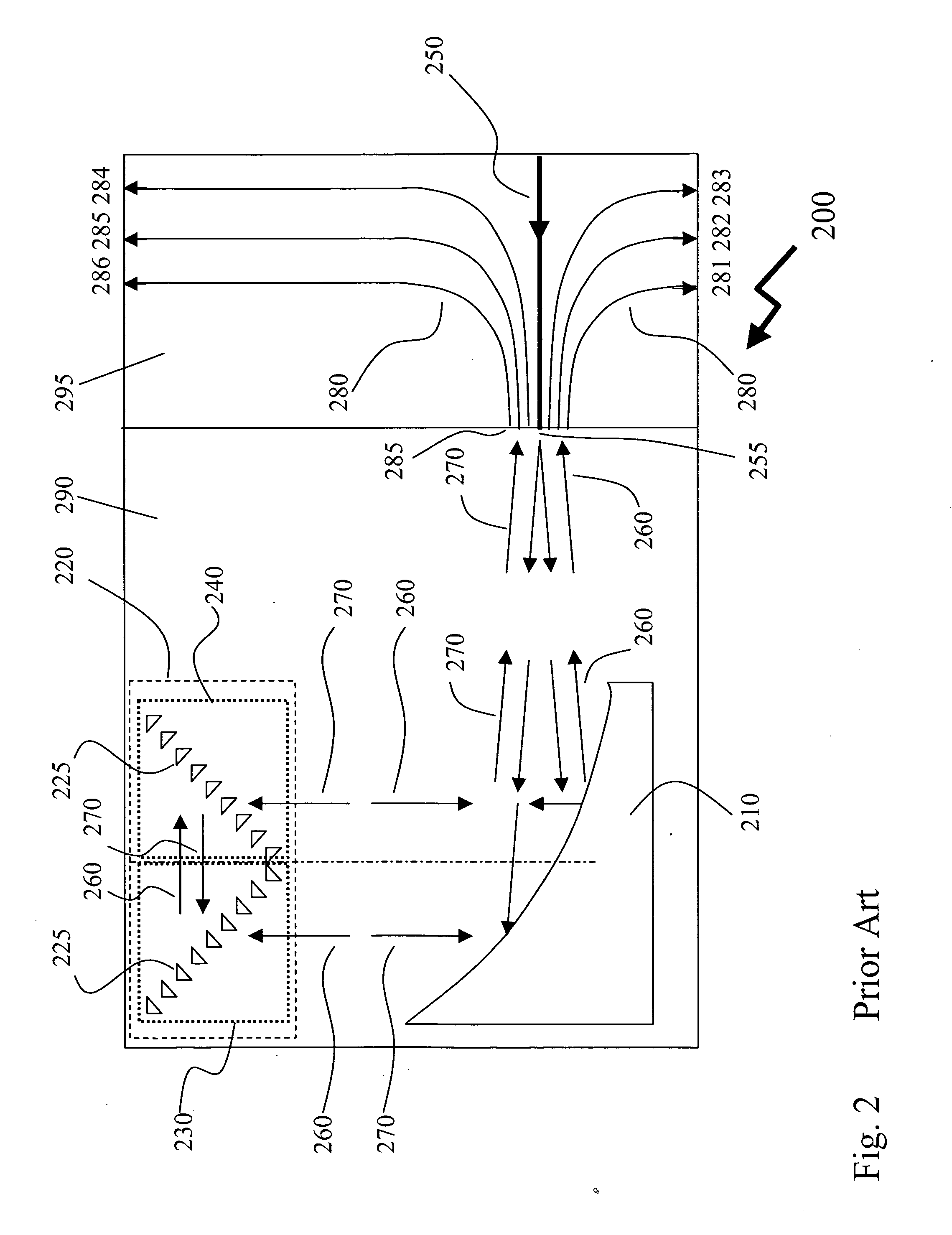
However, they suffer from being discrete passive components that cannot be integrated into a monolithic device for PICs, and involve precise alignment and assembly which becomes very difficult when channel counts increase and tens of optical fibers are aligned to the grating focal plane.
All of these constraints further making the etching process complex, expensive and low yield.
However, the multiple materials typically present within the InP / InGaAsP and GaAs / AlGaAs structures present additional processing complexities as the etch chemistry employed must work on many materials including in some designs layers normally added to provide etch stops within the structure for easing manufacturing tolerances.

Method used


Image

  • Integrated etched multilayer grating based wavelength demultiplexer
  • Integrated etched multilayer grating based wavelength demultiplexer
  • Integrated etched multilayer grating based wavelength demultiplexer

Examples


first embodiment

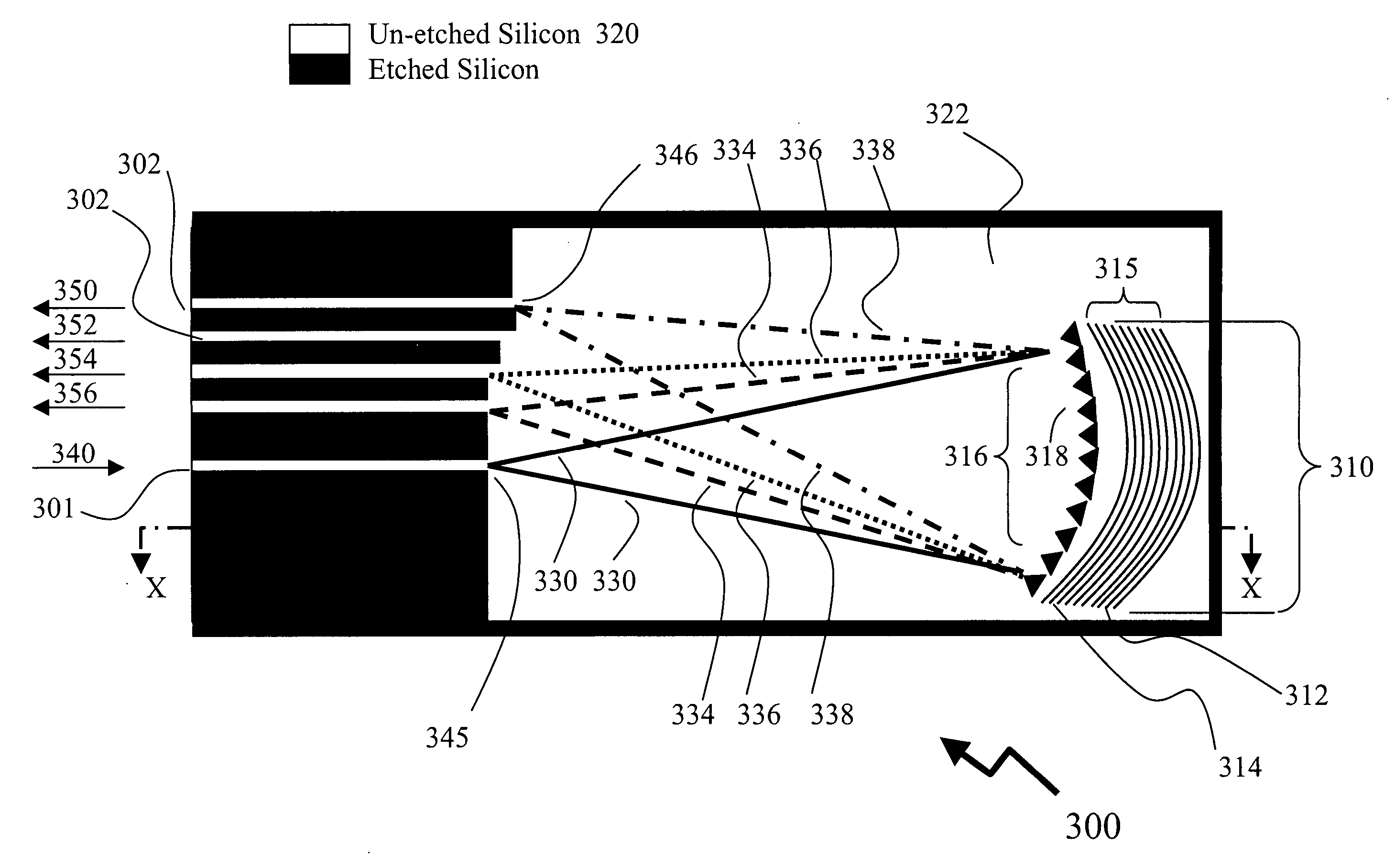
[0048]FIG. 3 is an exemplary schematic representation of the invention depicting an echelette multilayer diffraction grating-based wavelength demultiplexer (MLDG-WDM) 300. As shown the MLDG-WDM 300 is generally comprised of a common channel waveguide 301, a plurality of wavelength channel waveguides 302, and the multi-layer diffraction grating (MLDG) 310. In common with previous descriptions operation of the MLDG-WDM 300 will be described as a demultiplexer, although the device may be reversed and be used as a multiplexer, without departing from the general scope and nature of the present disclosure. Other such applications for the MLDG-WDM 300 may include, but are not limited to, spectrometers, spectro-transducers, optical routers, reconfigurable optical add-drop multiplexers (ROADM), optical cross-connects, fixed optical add-drop multiplexers, band multiplexers, and optical interleavers. The following discussion will generally focus on the use of MLDG-WDM 300, and its alternative ...

second embodiment

[0061]FIG. 5 is an exemplary schematic representation of the invention depicting an echelle MLDG-WDM 500 employing an echelle multilayer grading-based wavelength demultiplexer (echelle MLDG) 510. The echelle based MLDG-WDM 500 comprises a monolithically integrated structure 502 comprised of a common wavelength waveguide 550, a plurality of wavelength channel waveguides 552, and the echelle MLDG 510.

[0062] The common wavelength waveguide 550 and plurality of wavelength channel waveguides 552 are again generally comprised of equal depth ridges ( 50-100 nm high) in which light is guided through a waveguiding effect. That is, an input beam 530 coupled from an input optical fibre, or similar optical coupling arrangement (not shown for clarity) is launched into the common wavelength channel waveguide 550 and is guided thereby toward the multilayer grating structure 510. Likewise, output wavelength signals 542 through 548, after being reflectively diffracted by the echelle MLDG 510 and dir...


PUM


Abstract

An integrated etched multilayer grating-based wavelength multiplexer / demultiplexer is disclosed wherein an etched multilayer grating structure is monolithically integrated within the optical waveguide stack of the multiplexer / demultiplexer to reflectively diffract an input optical beam. The multilayer grating structure is generally comprised of a series of etched diffractive elements and an etched multilayer reflector, the combined optical response of which providing the desired multiplexing / demultiplexing effect. The etched structures are generally comprised of shallow etch structures in a top surface of the multiplexer / demultiplexer waveguide stack. Monolithically integrated input and output ridge waveguides may also be provided, optionally fabricated in a same etching step as the etched multilayer grating.

Description

[0001] This application claims priority from U.S. patent application Ser. No. 60 / 727,879 filed Oct. 19, 2005, the entire contents of which are incorporated herein by reference. FIELD OF THE INVENTION [0002] The invention relates to integrated optical wavelength multiplexer and de-multiplexers and, more particularly to providing integrated etched multilayer grating structures for wavelength dispersive elements. BACKGROUND OF THE INVENTION [0003] Driven by bandwidth hungry applications, optical broadband access networks have advanced very rapidly in recent years, becoming the core of new triple-play telecommunication services, which deliver data, video and voice on the same optical fiber right to the user. Deep penetration of the optical fiber into the access networks is accompanied with massive deployment of the optical gear that drives data traffic along the fiber links. The result is that wavelength division multiplexed optical networks which receive downstream and send upstream da...

Claims


Application Information

Patent Timeline
IPC IPC(8): G02B6/34
CPCG02B6/12007G02B6/124G02B6/29326G02B6/29328G02B6/2938
Inventor KIRK, ANDREW G.BISAILLON, ERIC
Owner MCGILL UNIV
Learn More