
Multi-port memory device with serial input/output interface

a multi-port memory and serial input technology, applied in the direction of information storage, static storage, digital storage, etc., can solve the problems of difficult to verify the operation of the multi-port memory device, the limitation of the conventional test device for testing the typical dram device in transferring and recognizing high-speed data signals, and the increase of the manufacturing cos

Active Publication Date: 2007-03-29
SK HYNIX INC
View PDF11 Cites 17 Cited by
  • Summary
  • Abstract
  • Description
  • Claims
  • Application Information

AI Technical Summary

Benefits of technology

[0030] It is, therefore, an object of the present invention to provide a multi-port memory device capable of performing high-speed test operation by using a test device for performing low-speed test operation in a parallel I / O interface.

Problems solved by technology

Consequently, as distance increases, the manufacturing cost increases.
In this case, a conventional test device for testing the typical DRAM device has a limitation in transferring and recognizing high-speed data signals.
Accordingly, it is difficult to verify an operation of the multi-port memory device so that a test device for high-speed is required.
However, since a large investment is required to introduce the test device for high-speed, the unit cost of production is increased and a competitiveness of the product is weakened accordingly.

Method used


Image

  • Multi-port memory device with serial input/output interface
  • Multi-port memory device with serial input/output interface
  • Multi-port memory device with serial input/output interface

Examples


first embodiment

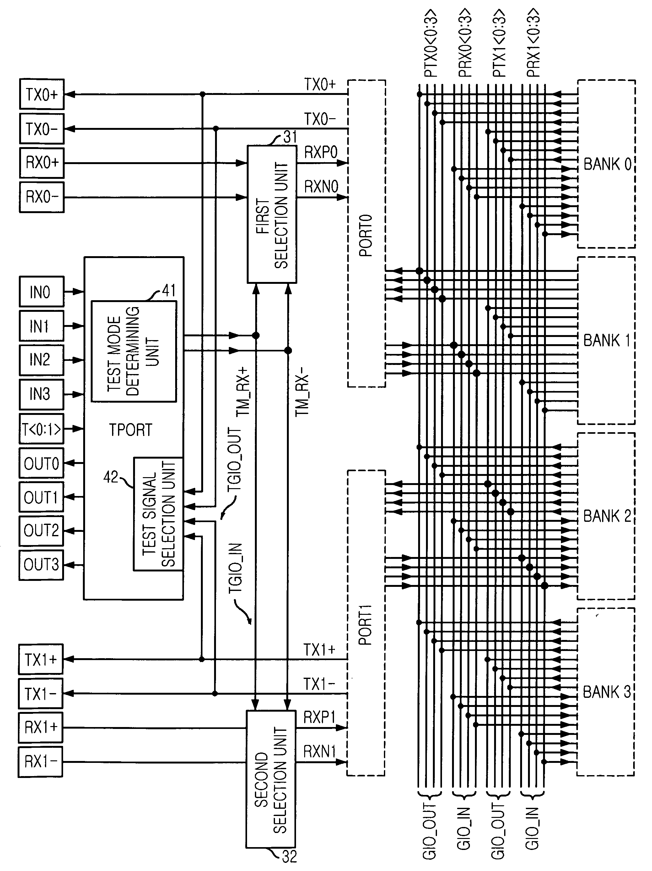
[0048]FIG. 3 is a block diagram of a multi-port memory device in accordance with the present invention. For convenience of explanation, the multi-port memory device having two ports and four banks is illustrated.

[0049] The multi-port memory device includes a plurality of serial I / O pads TX0+, TX0+, TX1+, TX1−, RX0+, RX0−, RX1+ and RX1−, a plurality of parallel I / O pads IN, T and OUT, a test port TPORT, first and second selection units 31 and 32, first and second ports PORT0 and PORT1, first to fourth banks BANK0 to BANK3, and first and second global input / output (I / O) data buses GIO_IN and GIO_OUT.

[0050] The plurality of serial I / O pads support data communication between the first and second ports PORT0 and PORT1 and external devices in high-speed serial I / O interface. The serial I / O pads include transmission pads such as TX0+, TX0−, TX1+ and TX1− and reception pads such as RX0+, RX0−, RX1+ and RX1−. The transmission pads TX0+, TX0−, TX1+ and TX1− transfer output valid data signals...

second embodiment

[0120] Meanwhile, in accordance with the second embodiment, the test data output unit 435 of the test port TPORT shown in FIG. 4 includes an output driver which becomes a high impedance state during the normal mode so as not to transfer any signals to the transmission pads TX0+, TX0−, TX1+ and TX1−. Accordingly, the output driver may operate in response to the inverted test mode enable signal TMENB.

[0121] The first and second global I / O data buses GIO_IN and GIO_OUT shown in FIGS. 3 and 10 may include a latch for stably transferring signals between the ports and the banks.

[0122] For convenience of explanation, in the first and second embodiments of the present invention, the unit of processing data is set to 4-bit unit. Accordingly, the multi-port memory device of the first and second embodiments allocates four global I / O data buses per each port. Further, the multi-port memory device in accordance with the first embodiment includes four parallel I / O pads. However, the number of th...


PUM


Abstract

A multi-port memory device includes a plurality of serial I / O data pads; a plurality of parallel I / O data pads; a plurality of first ports for performing a serial I / O data communication with external devices through the serial I / O data pads; a plurality of banks for performing a parallel I / O data communication with the first ports via a plurality of first data buses; and a second port for performing a parallel I / O data communication with the external devices through the parallel I / O data pads and a serial I / O data communication with the first ports via a plurality of second data buses, during a test mode.

Description

FIELD OF THE INVENTION [0001] The present invention relates to a multi-port memory device, and more particularly, to a test interface of a multi-port memory device with a serial input / output (I / O) interface for processing a multiple concurrent operation with external devices. DESCRIPTION OF RELATED ARTS [0002] Generally, most memory devices including random access memory (RAM) have a single port with a plurality of input / output pin sets. That is, the single port is provided for data exchange between a memory device and an external chipset. Such a memory device having the single port uses a parallel input / output (I / O) interface to simultaneously transmit multi-bit data through signal lines connected to a plurality of input / output (I / O) pins. The memory device exchanges data with the external device through a plurality of I / O pins in parallel. [0003] The I / O interface is an electrical and mechanical scheme to connect unit devices having different functions through signal lines and tra...

Claims


Application Information

Patent Timeline
Patent Type & Authority Applications(United States)
IPC IPC(8): G11C8/00
CPCG11C8/16G11C29/48G11C29/32G11C29/1201
Inventor DO, CHANG-HO
Owner SK HYNIX INC
Learn More