Array substrate of liquid crystal display device and method of fabricating the same

a liquid crystal display and array substrate technology, applied in semiconductor devices, instruments, electrical equipment, etc., can solve the problems of disadvantages of lcd devices and problems with driving lcd devices, and achieve the effects of improving structure, and preventing electrical short circuits

Active Publication Date: 2007-03-29
LG PHILIPS LCD CO LTD
View PDF7 Cites 4 Cited by
  • Summary
  • Abstract
  • Description
  • Claims
  • Application Information

AI Technical Summary

Benefits of technology

[0016] An object of the present invention is to provide an array substrate of a liquid crystal display device having an improved structure to prevent electrical short circuiting between a drain electrode and a data line.
[0017] Another object of the present invention is to provide a method of fabricating an array substrate of a liquid crystal display device to prevent electrical short circuiting between a drain electrode and a data line.

Problems solved by technology

However, the LCD devices are disadvantageous due to their narrow viewing angle.
Thus, driving the LCD device may be problematic due to the electrical short circuit of the data line 24 and the drain electrode 28.

Method used


Image

  • Array substrate of liquid crystal display device and method of fabricating the same
  • Array substrate of liquid crystal display device and method of fabricating the same
  • Array substrate of liquid crystal display device and method of fabricating the same

Examples


Embodiment Construction

[0033] Reference will now be made in detail to the illustrated embodiments of the present invention, which are illustrated in the accompanying drawings.

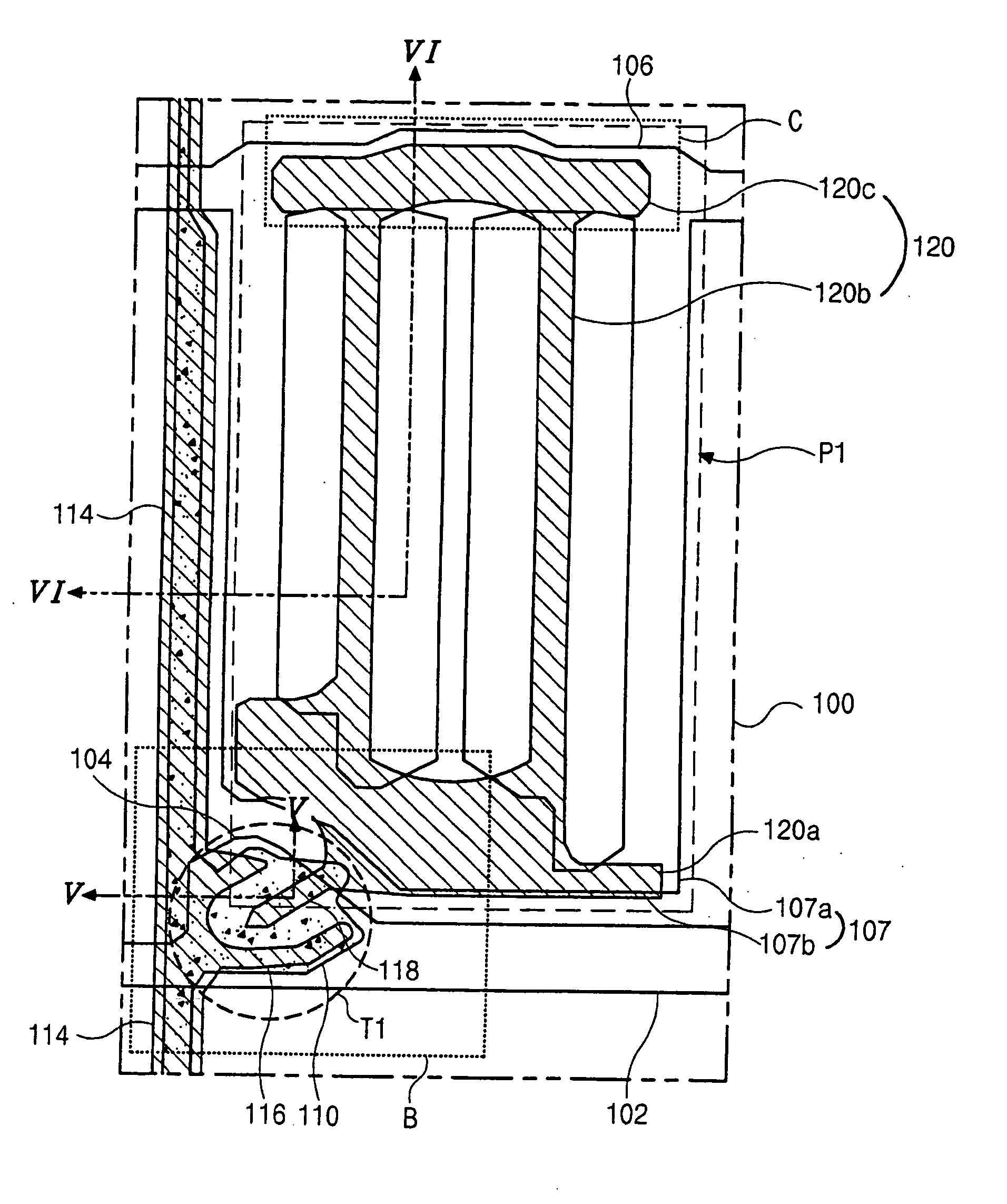
[0034]FIG. 3 is a plan view of an exemplary array substrate for an IPS LCD device according to the present invention. In FIG. 3, a gate line 102 may be formed along a first direction on a substrate 100, and a common line 106 may be formed along the first direction parallel to the gate line 102 on the substrate 100. In addition, a data line 114 may be formed on the substrate 100 along a second direction perpendicular to the first direction to cross the gate line 102 and the common line 106, wherein the data line 114 and the gate line 102 may define a pixel area P1.

[0035] A thin film transistor T1 may be formed at the crossing of the gate and data lines 102 and 114 to function as a switching element. The thin film transistor T1 may include a gate electrode 104 that may be connected to the gate line 102, a source electrode 116 that ma...


PUM

PropertyMeasurementUnit
lengthaaaaaaaaaa
lengthaaaaaaaaaa
semiconductoraaaaaaaaaa

Abstract

An array substrate of a liquid crystal display device includes a substrate, a gate line and a data line on the substrate, the gate line and the data line crossing each other to define a pixel area, a common line parallel to the gate line, a common electrode extending from the common line and including a plurality of vertical portions, a thin film transistor electrically connected to the gate line and the data line, the thin film transistor including a gate electrode connected to the gate line, a semiconductor layer over the gate electrode, a source electrode over the semiconductor layer and connected to the data line, and a drain electrode over the semiconductor layer and spaced apart from the source electrode, wherein a portion of the semiconductor layer partly covers a side of the gate electrode disposed between the data line and the drain electrode, and a pixel electrode in the pixel area, the pixel electrode connected to the drain electrode, and includes a plurality of vertical parts alternating with the plurality of vertical portions of the common electrode.

Description

[0001] The present invention claims the benefit of Korean Patent Application No. 2002-60706, filed in Korea on Oct. 4, 2002, which is hereby incorporated by reference. BACKGROUND OF THE INVENTION [0002] 1. Field of the Invention [0003] The present invention relates to a liquid crystal display (LCD) device and method of fabricating a liquid crystal display device, and more particularly, to an array substrate of a liquid crystal display device and a method of fabricating an array substrate of a liquid crystal display device. [0004] 2. Discussion of the Related Art [0005] In general, liquid crystal display (LCD) devices are driven by making use of optical anisotropy and polarization characteristics of a liquid crystal material. The LCD devices commonly include two substrates that are spaced apart and face each other, and a liquid crystal material layer interposed between the two substrates. Each of the substrates includes electrodes that face each other, wherein a voltage supplied to e...

Claims


Application Information

Patent Timeline
Patent Type & Authority Applications(United States)
IPC IPC(8): H01L29/04G02F1/136G02F1/1343G02F1/1362G02F1/1368
CPCG02F1/134363G02F2001/136295G02F1/1368G02F1/136295G02F1/136
Inventor KIM, HEUNG-SOO
Owner LG PHILIPS LCD CO LTD
Why Eureka
Try Eureka