Semiconductor display device and method of driving a semiconductor display device
a display device and semiconductor technology, applied in the direction of instruments, computing, electric digital data processing, etc., can solve the problems of screen flicker, increased cost, and the drive frequency of the electronic device that generates the image signal cannot handle the image signal frequency, so as to prevent the generation of stripes, the effect of increasing frame frequency and preventing the reduction of the brightness of the overall display screen
- Summary
- Abstract
- Description
- Claims
- Application Information
AI Technical Summary
Benefits of technology
Problems solved by technology
Method used
Image
Examples
embodiment 1
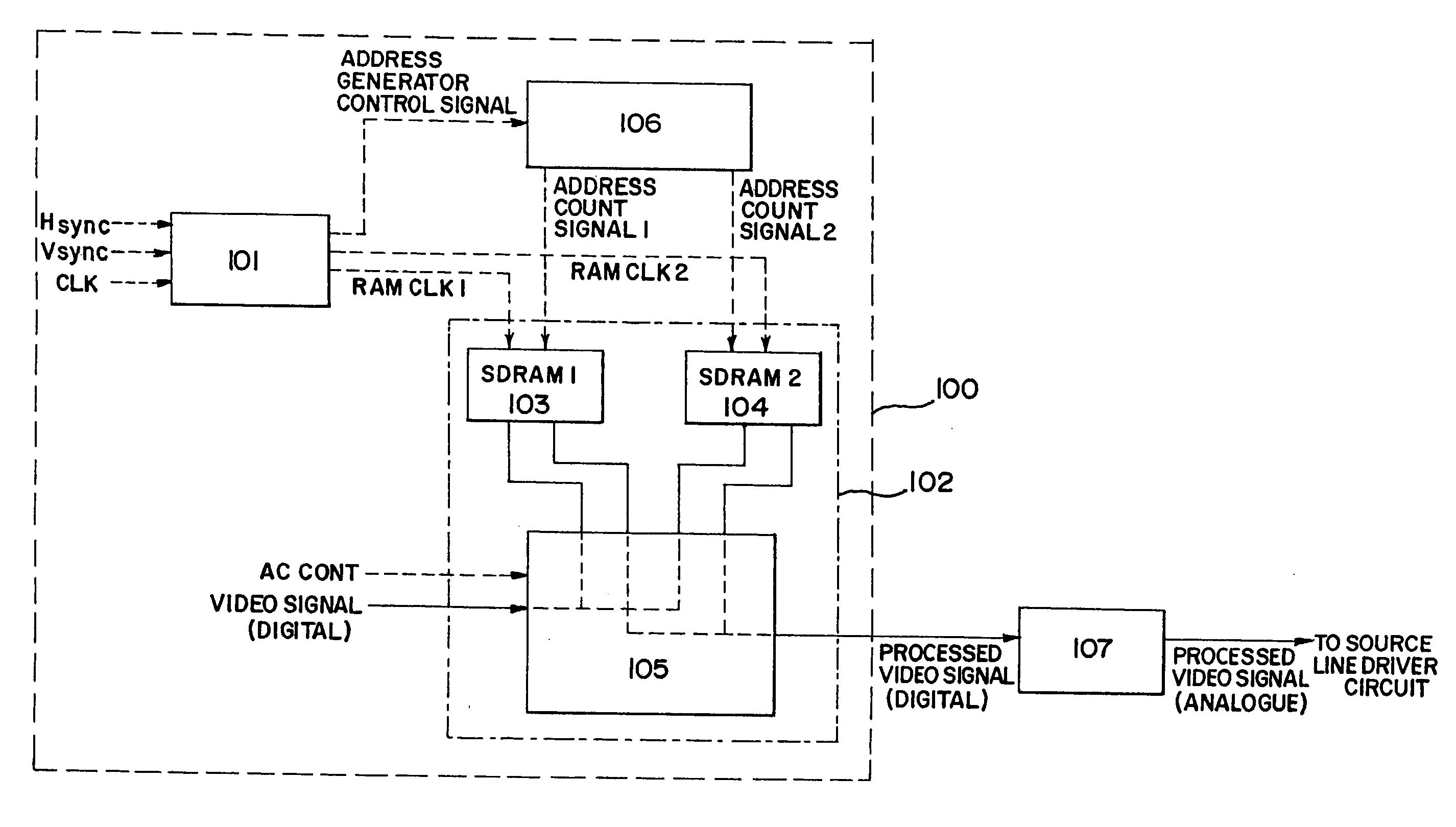
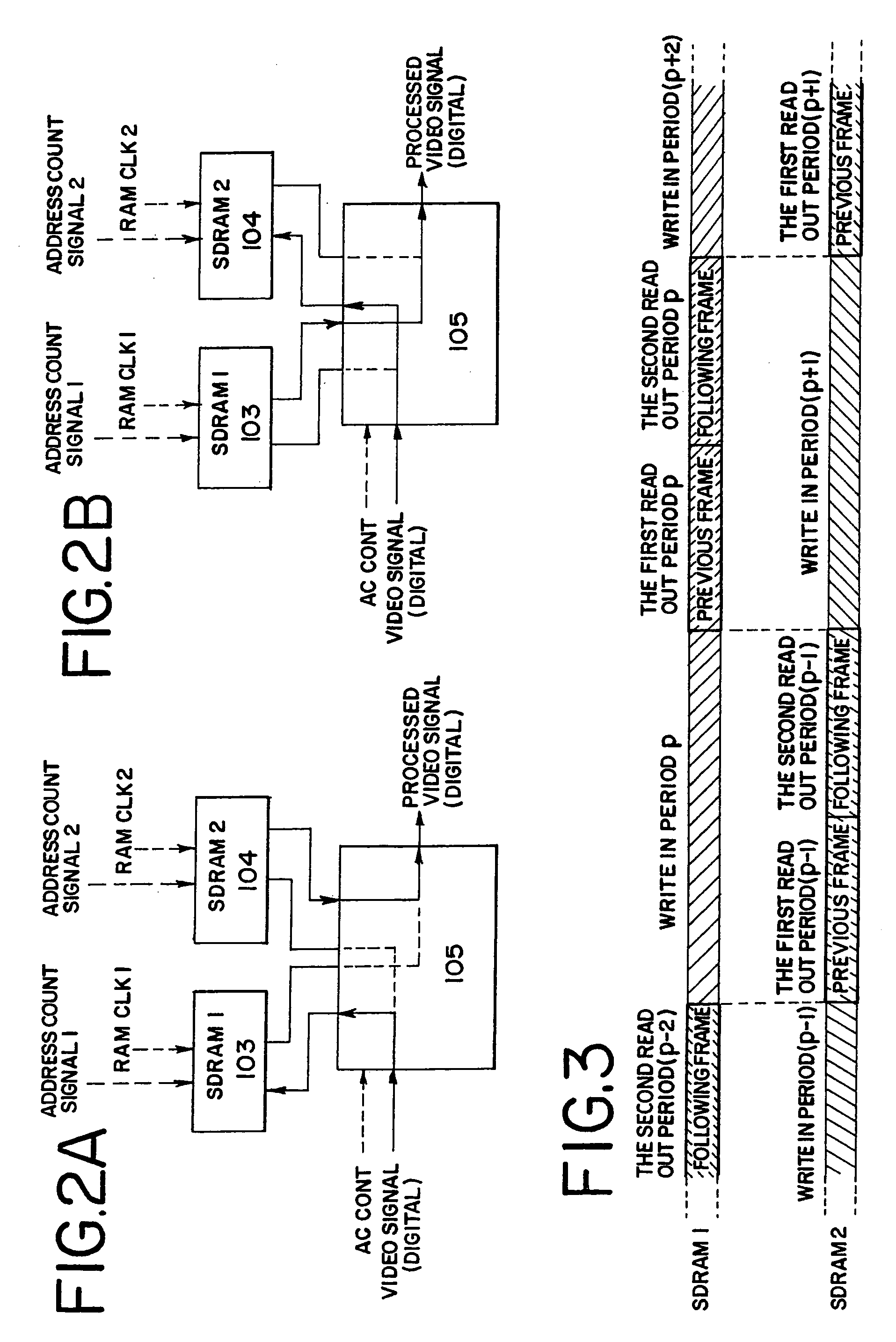
[0305] Input and output timing of an image signal in the first SDRAM 103 and the second SDRAM 104 of FIG. 1 are explained in Embodiment 1 using an example which differs from that of FIG. 3.
[0306] The first and the second read out periods are shorter than the write in period in Embodiment 1. A blank period during which write in and read out of the image signal is not performed is then provided after completion of a first and a second read out periods and before the start of a next write in period.
[0307] Image signal write in and read out timing for the first SDRAM 103 and the second SDRAM 104 is shown in FIG. 10. The image signal is written to the first SDRAM 103 in the write in period p. The image signal-input to the first SDRAM 103 in a write in period p is then read out two times, in a first read out period p and in a second read out period p.
[0308] Further, the image signal is written to the second SDRAM 104 in a write in period (p−1). The image signal input to the second SDRA...
embodiment 2
[0315] Input and output timing of an image signal in the first SDRAM 103 and the second SDRAM 104 of FIG. 1 are explained in Embodiment 2 using an example which differs from that of FIG. 3 and FIG. 10.
[0316] The first and the second read out periods are longer than the write in period in Embodiment 2. A blank period during which write in and read out of the image signal is not performed is then formed after completion of the write in period and before the start of a next is first read out period.
[0317] Image signal write in and read out timing for the first SDRAM 103 and the second SDRAM 104 is shown in FIG. 11. The image signal is written to the first SDRAM 103 in a write in period p. A blank period appears after the write in period p. The blank period is a period during which write in and read out of the image signal is not performed.
[0318] The image signal input to the first SDRAM 103 in the write in period p is then read out two times, in a first read out period p and in a se...
embodiment 3
[0327] An example of a frame rate conversion portion, differing from that of FIG. 1, of a semiconductor display device of the present invention is explained in Embodiment 3 using FIG. 12.
[0328] The frame rate conversion portion has there SDRAMs in Embodiment 3.
[0329] A frame rate conversion portion 200 has a control portion 201, a frame frequency conversion portion 202, and an address generator portion 206. Further, the frame frequency conversion portion 202 has a first SDRAM (SDRAM 1) 203, a second SDRAM (SDRAM 2) 204, a third SDRAM (SDRAM 3) 207, and a date format portion 205. Reference numeral 208 denotes a D / A converter circuit, which converts an image signal output from the frame rate conversion portion 200 from digital to analog.
[0330] Note that although the frame frequency conversion portion 202 has three SDRAMs (the first SDRAM 203, the second SDRAM 204, and the third SDRAM 207) in Embodiment 3, the number of SDRAMs is not limited to three.
[0331] An Hsync signal, a Vsync...
PUM
 Abstract
Description
Claims
Application Information
 - R&D
- Intellectual Property
- Life Sciences
- Materials
- Tech Scout
- Unparalleled Data Quality
- Higher Quality Content
- 60% Fewer Hallucinations
Browse by: Latest US Patents, China's latest patents, Technical Efficacy Thesaurus, Application Domain, Technology Topic, Popular Technical Reports.
© 2025 PatSnap. All rights reserved.Legal|Privacy policy|Modern Slavery Act Transparency Statement|Sitemap|About US| Contact US: help@patsnap.com


