Interposers with alignment fences and semiconductor device assemblies including the interposers

a technology of alignment fences and semiconductor devices, applied in the direction of electrical apparatus construction details, instruments, measurement instrument housings, etc., can solve the problems of electrical shorts between adjacent bond wires, significant number of semiconductor devices to fail, and penetration of particulate die coats, so as to facilitate some movement of semiconductor devices

Inactive Publication Date: 2006-12-14
AKRAM SALMAN +2
View PDF80 Cites 4 Cited by
  • Summary
  • Abstract
  • Description
  • Claims
  • Application Information

AI Technical Summary

Benefits of technology

[0022] The interposer of the present invention includes a semiconductor (e.g., silicon or ceramic) substrate having contact pads on a top side thereof and arranged correspondingly to conductive structures, such as solder bumps, protruding from a semiconductor device to be tested. A conductive via connects each contact pad on the top side of the interposer to a conductive element, such as a contact pad on the bottom side thereof or an electrically conductive pin, to facilitate connection with a tester. Electrical traces may reroute the positions of one or more of the contact pads from the top side to the bottom side of the interposer. The contact pads on the bottom side of the interposer are arranged correspondingly to test pads or test sockets of a test substrate with which the interposer is to be used. Conductive structures protrude from the contact pads on the bottom side of the interposer to facilitate electrical communication between the contact pads on the bottom of the interposer and their corresponding test pads or sockets.
[0026] In another aspect, the raised periphery of the fence of the present invention includes laterally recessed regions that are facing, but spaced apart from, a semiconductor device when disposed in the receptacle. These laterally recessed regions facilitate some movement of a semiconductor device within the receptacle. Thus, a fence including such lateral recesses may be the to roughly align a semiconductor device disposed in the receptacle thereof, rather than precisely aligning the semiconductor device. When a semiconductor device is inserted into the receptacle of a fence having lateral recesses in the raised periphery thereof, fine alignment occurs as the conductive structures of the semiconductor device are received within apertures of the fence or recesses through which the contact pads on the top of the interposer are exposed.

Problems solved by technology

However, it is now recognized that conventional packaging processes may cause significant numbers of semiconductor devices to fail.
For example, as a semiconductor device is being encapsulated, the protective material may cause particulate die coat penetration, “bond wire sweep,” which may break electrical connections made by the bond wires or cause electrical shorts between adjacent bond wires, and other problems.
Some state of the art semiconductor devices lack conventional packages (e.g., leads and encapsulants) or are minimally packaged.
When these types of semiconductor devices are tested, the solder bumps or other conductive structures protruding therefrom may not properly align with the corresponding test sockets of a test substrate so as to establish adequate electrical contacts between the tested semiconductor device and the test substrate.
Moreover, if misalignment occurs, the conductive structures may be damaged.
Nonetheless, the conductive structures protruding from a semiconductor device to be tested may be damaged when assembled with such an interposer.
Moreover, since the recesses of such interposers are configured to receive the conductive structures of a semiconductor device without stressing, deforming, or otherwise damaging the conductive structures, the interposer may fail to make adequate electrical connections between some of the conductive structures and their corresponding test pads or sockets of the test substrate.
Moreover, test interposers typically lack any alignment component other than the recesses thereof.
Accordingly, it appears that the art is lacking a structure for aligning the conductive structures of a semiconductor device with corresponding test pads or sockets of a test substrate without stressing or damaging the conductive structures while facilitating adequate electrical connections between the conductive structures and the test pads or sockets.
However, to the inventors' knowledge, stereolithography has yet to be applied to mass production of articles in volumes of thousands or millions, or employed to produce, augment or enhance products including other pre-existing components in large quantities, where minute component sizes are involved, and where extremely high resolution and a high degree of reproducibility of results are required.
Furthermore, conventional stereolithography apparatus and methods fail to address the difficulties of precisely locating and orienting a number of pre-existing components for stereolithographic application of material thereto without the use of mechanical alignment techniques or to otherwise assure precise, repeatable placement of components.
In particular, stereolithography has not been employed to fabricate interposers for aligning and connecting a semiconductor device to a test substrate.

Method used


Image

  • Interposers with alignment fences and semiconductor device assemblies including the interposers
  • Interposers with alignment fences and semiconductor device assemblies including the interposers
  • Interposers with alignment fences and semiconductor device assemblies including the interposers

Examples


Embodiment Construction

The Interposer

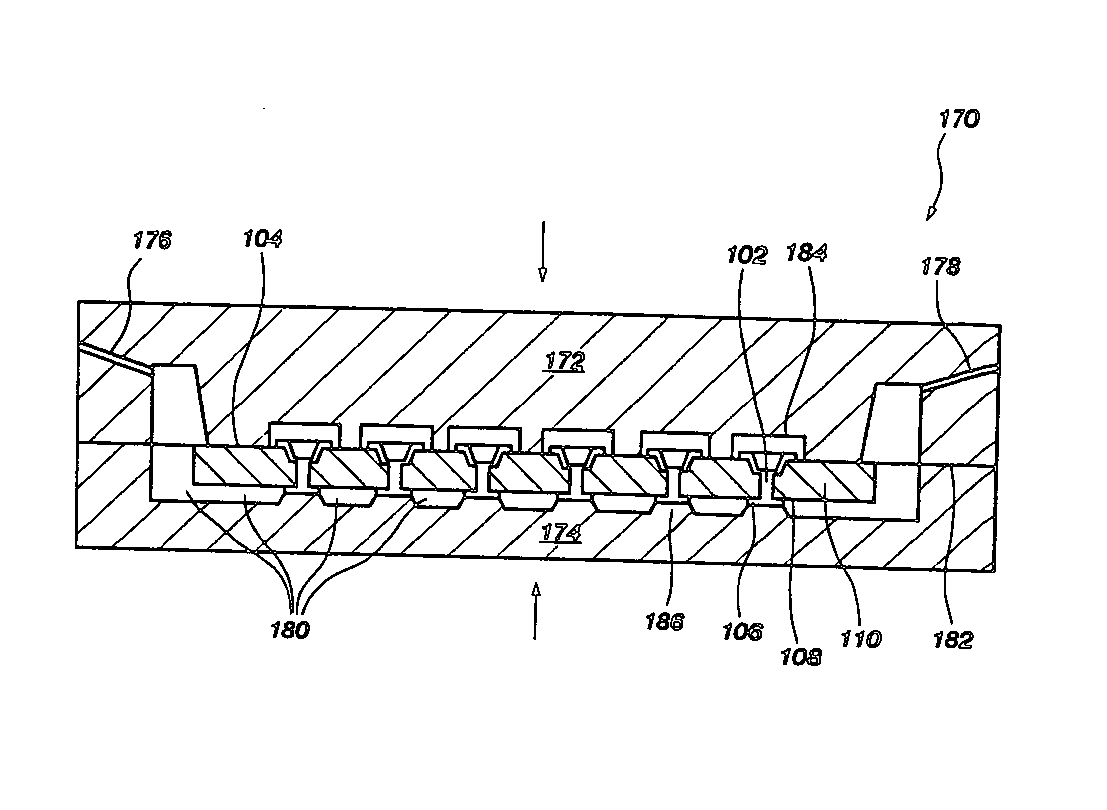
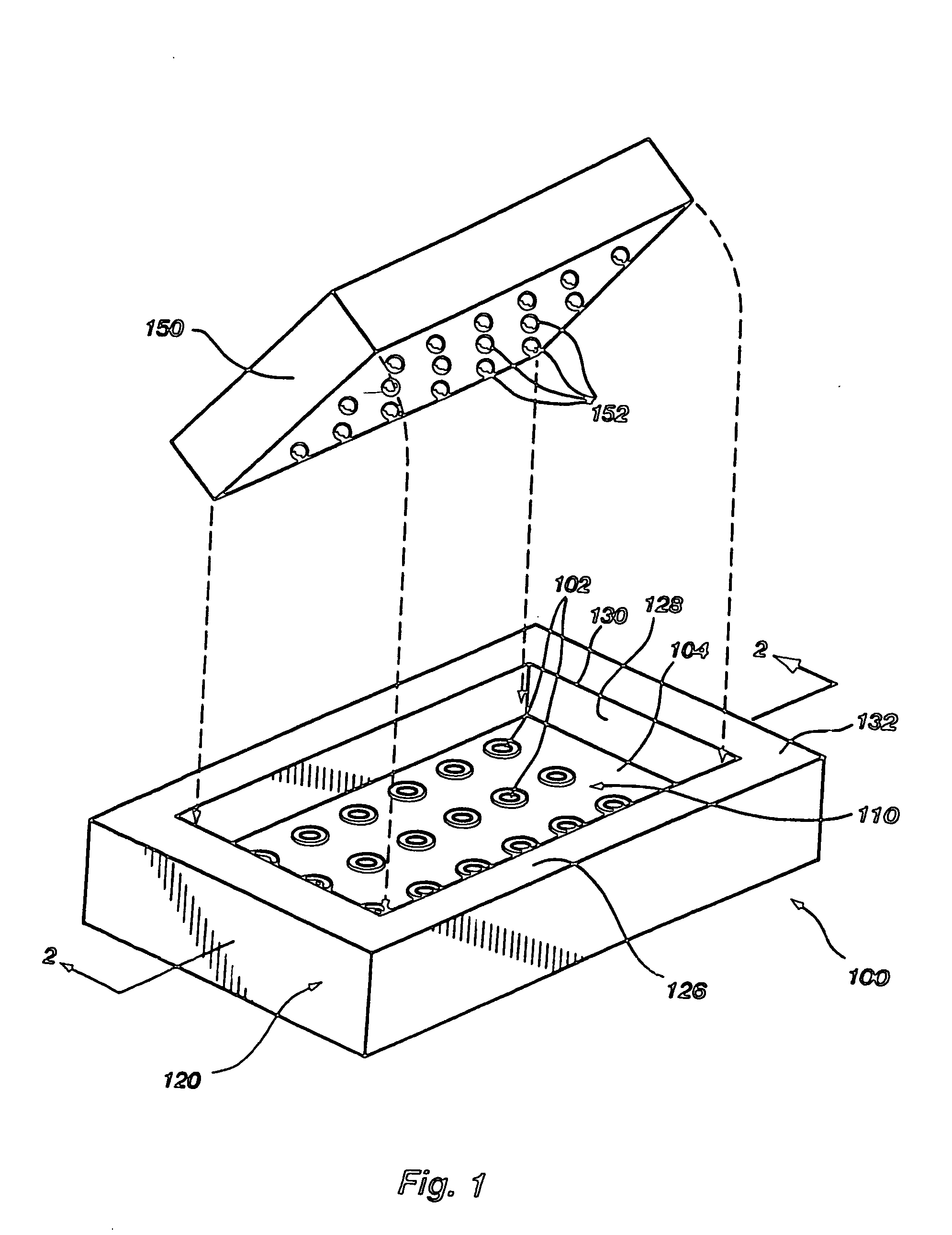
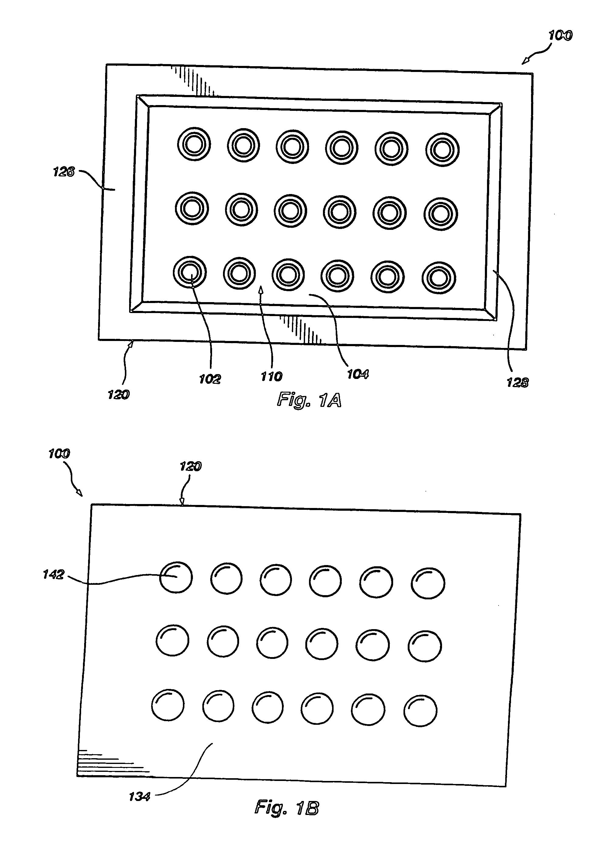
[0049]FIGS. 1, 1A, 1B, and 2 depict an exemplary interposer 100 of the present invention. Interposer 100 includes an interposer substrate 110 with contact pads 102 on a top surface 104 thereof and contact pads 106 on a bottom surface 108 thereof. Contact pads 102 may be recessed relative to top surface 104, as illustrated in FIG. 2. Contact pads 102 on top surface 104 of interposer substrate 110 communicate with corresponding contact pads 106 on bottom surface 108 by way of vias 118 filled or lined with metal 148 or another conductive material. Conductive structures 142, such as balls, bumps, or conductive pillars, of a conductive material, such as a solder, a metal, a metal alloy, a conductor-filled epoxy, a conductive epoxy, or a conductive (e.g., z-axis) elastomer, are secured to and protrude from contact pads 106 and from interposer 100.

[0050] Interposer substrate 110 may be fabricated from any suitable material for use in semiconductor device applications, such ...


PUM

PropertyMeasurementUnit
thickaaaaaaaaaa
thicknessaaaaaaaaaa
sizeaaaaaaaaaa

Abstract

An interposer includes a fence that orients or aligns a semiconductor device, such as a flip-chip type semiconductor device, with an interposer substrate. The fence may include edges that are configured to progressively align a semiconductor device with the interposer substrate. The fence may also include one or more laterally recessed regions to facilitate rough alignment of a semiconductor device with the interposer substrate. The fence may comprise a unitary structure or a plurality of mutually adhered regions.

Description

CROSS-REFERENCE TO RELATED APPLICATIONS [0001] This application is a continuation of application Ser. No. 10 / 648,163, filed Aug. 26, 2003, pending, which application is a continuation of application Ser. No. 09 / 843,119, filed Apr. 26, 2001, now U.S. Pat. No. 6,634,100, issued Oct. 21, 2003, which is a divisional of application Ser. No. 09 / 533,407, filed Mar. 23, 2000, now U.S. Pat. No. 6,529,027, issued Mar. 4, 2003.BACKGROUND OF THE INVENTION [0002] 1. Field of the Invention [0003] The present invention relates generally to an interposer configured to receive a semiconductor device for testing. More specifically, the invention pertains to such a test interposer having an alignment fence for receiving and aligning semiconductor devices, such as flip-chip type semiconductor dice, ball grid array (BGA) packages, and chip scale packages (CSPs), with test sockets of the interposer. The present invention also relates to methods for fabricating such a test interposer. [0004] 2. Background...

Claims


Application Information

Patent Timeline
Patent Type & Authority Applications(United States)
IPC IPC(8): H05K7/00G01R1/04H05K1/11H05K1/14H05K3/34
CPCG01R1/0408Y10T29/4913G01R1/0466G01R1/0483G01R1/07378G01R3/00H01L23/32H01L23/49827H01L24/72H01L2224/16H01L2924/01049H01L2924/01082H01L2924/12044H05K1/112H05K1/141H05K3/3436H05K7/1061H05K2201/049H05K2201/09472H05K2201/10378H05K2201/10734H05K2201/2018H05K2203/167H01L2924/01005H01L2924/01006H01L2924/01033H01L2224/16225H01L2224/16237H01L2224/8114Y10T29/49144Y10T29/49156Y10T29/49218Y10T29/49165Y10T29/49126Y10T29/49147Y10T29/49222Y10T29/49204G01R1/0433B33Y10/00B33Y30/00B33Y80/00H01L2224/16111H01L2224/81385H01L2924/12042H01L2924/15787H01L2924/351H01L2924/00
Inventor AKRAM, SALMANWOOD, ALAN G.FARNWORTH, WARREN M.
Owner AKRAM SALMAN
Why Eureka
Try Eureka