Method for assembling testing equipment for semiconductor substrate
a technology for semiconductor substrates and testing equipment, which is applied in the direction of individual semiconductor device testing, semiconductor/solid-state device testing/measurement, instruments, etc., can solve the problems of enormous assembly time, and achieve the effect of easy and accurate adjustment of the relative position of the probe pin
- Summary
- Abstract
- Description
- Claims
- Application Information
AI Technical Summary
Benefits of technology
Problems solved by technology
Method used
Image
Examples
first embodiment
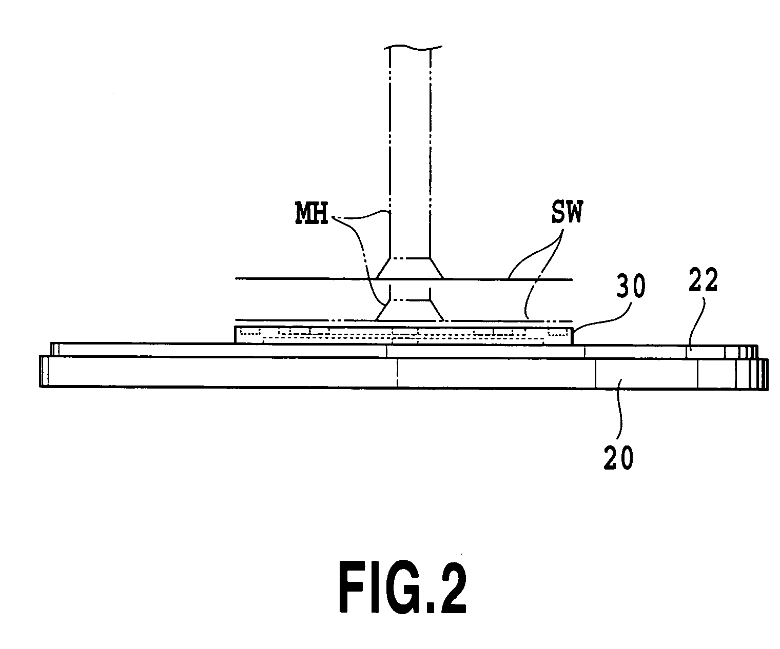
[0042]FIG. 2 schematically illustrates an overall structure of a probe head unit to which is applied the method for assembling a testing equipment for a semiconductor substrate in accordance with the present invention.
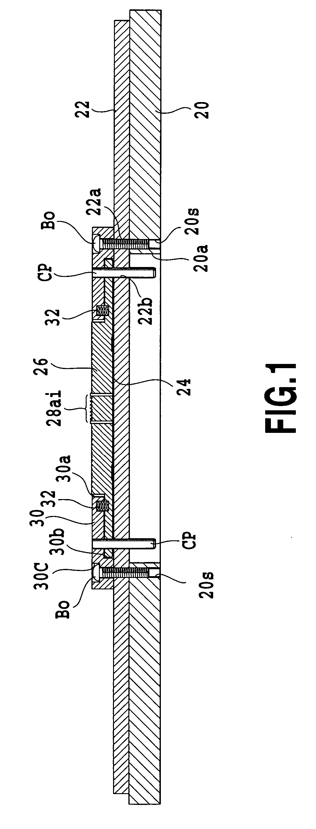
[0043] In FIG. 2, the probe head unit for the electric connection to a semiconductor substrate SW includes a reinforcement frame member 20 for reinforcing the rigidity of a printed wiring board 22, and a printed wiring board 22 as a test board for supplying test signals or others to circuit patterns in the tested semiconductor substrate SW disposed on one surface of the reinforcement frame member 20. As shown in FIG. 1, the probe head unit further includes a pitch-changing substrate 24 for the mutual electric connection between the printed wiring board 22 and a contact block 26 described later 26, the contact block 26 having a plurality of probe pins 28ai (i=1 to n, n is a positive integer) for the electric connection between the circuit patterns in the semiconductor s...
second embodiment
[0069]FIG. 9 schematically illustrates an overall structure of a probe head unit to which is applied the inventive method for assembling a testing equipment for a semiconductor substrate.
[0070] In the example shown in FIG. 1, the contact block 26 has the convex portion 26P and the flange portion 26F. Contrarily, in the example shown in FIG. 9, a contact block 36 has no such a flange portion, but, instead thereof, a dowel member 38 is disposed on the pitch-changing substrate 24. In this regard, in the example shown in FIG. 9 and examples shown in FIGS. 10 to 19 described later, the same reference numerals are used for denoting the same elements and the explanation thereof will be eliminated.
[0071] The contact block 36 has a plurality of probe pins 36ai (i=1 to n, n is a positive integer) generally at a center thereof in correspondence to an electrode group 24E in the pitch-changing substrate 24 described above. Opposite ends of the probe pin 36ai penetrating the center are projected...
third embodiment
[0089]FIG. 12 schematically illustrates an overall structure of a probe head unit to which is applied the inventive method for assembling a testing equipment for a semiconductor substrate.
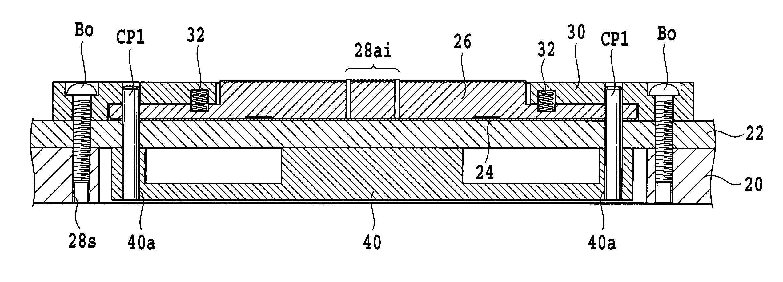
[0090] In the example shown in FIG. 9, the opening 20a in the reinforcement frame member 20 is a vacant space. Contrarily, in the example shown in FIG. 12, a second reinforcement frame member 40 is disposed in this space in accordance with the rigidity of the printed wiring board 22. In this regard, in FIGS. 12 to 15, the same reference numerals are used for denoting the same elements as in FIG. 9, and the explanation thereof will be eliminated.
[0091] The reinforcement frame member 40 has holes 40a at positions directly beneath the respective holes 22b in the printed wiring board 22, into which are inserted one ends of the respective positioning pins CP1. Thus, the one ends of the positioning pins CP1 are inserted into the holes 40a to further increase the rigidity of the printed wiring board 22. ...
PUM
| Property | Measurement | Unit |
|---|---|---|
| width | aaaaa | aaaaa |
| diameter | aaaaa | aaaaa |
| diameter | aaaaa | aaaaa |
Abstract
Description
Claims
Application Information
 - R&D
- Intellectual Property
- Life Sciences
- Materials
- Tech Scout
- Unparalleled Data Quality
- Higher Quality Content
- 60% Fewer Hallucinations
Browse by: Latest US Patents, China's latest patents, Technical Efficacy Thesaurus, Application Domain, Technology Topic, Popular Technical Reports.
© 2025 PatSnap. All rights reserved.Legal|Privacy policy|Modern Slavery Act Transparency Statement|Sitemap|About US| Contact US: help@patsnap.com


