Delay test method for large-scale integrated circuits

Inactive Publication Date: 2006-10-19
OKI ELECTRIC IND CO LTD
View PDF8 Cites 9 Cited by
  • Summary
  • Abstract
  • Description
  • Claims
  • Application Information

AI Technical Summary

Benefits of technology

[0034] An object of the present invention is to provide an accurate method of conducting a delay test of a large-scale integrated circuit.

Problems solved by technology

A general problem encountered when delay tests are carried out as described above is that a capture clock propagation delay may mask combinatorial logic delay faults.
It is possible to compensate for a moderate known capture clock delay β by shortening the launch-to-capture clock delay T, but this becomes impractical when β is very large, or is unknown.

Method used


Image

  • Delay test method for large-scale integrated circuits
  • Delay test method for large-scale integrated circuits
  • Delay test method for large-scale integrated circuits

Examples


Embodiment Construction

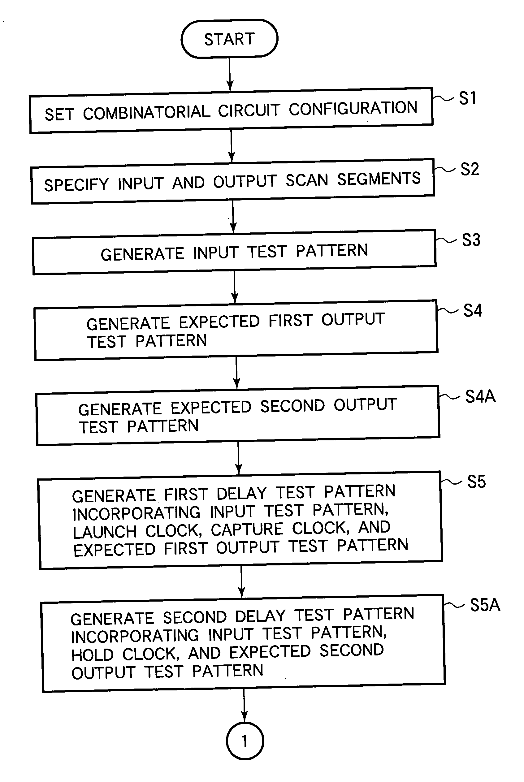
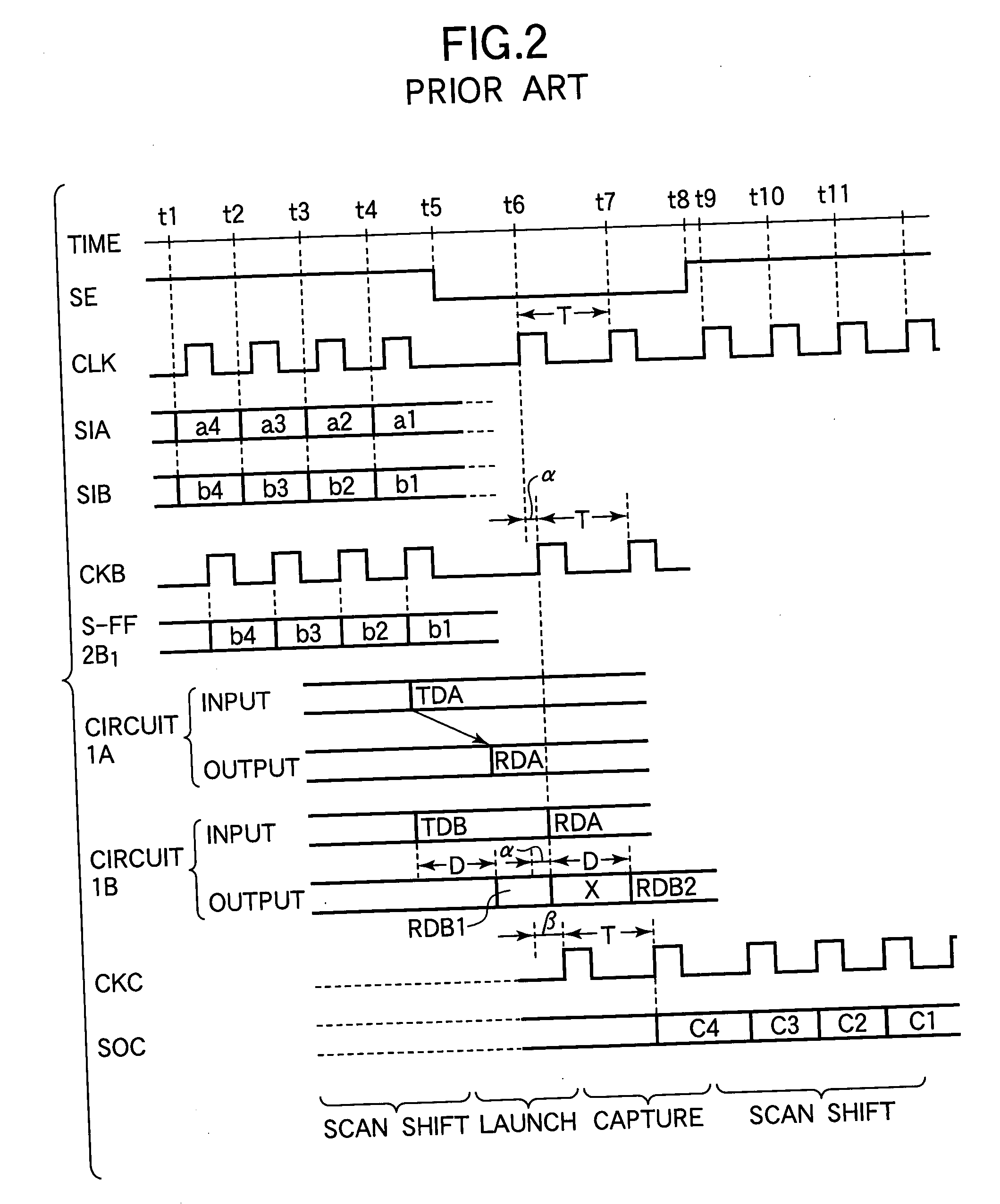
[0052] An embodiment of the invention will now be described with reference to FIGS. 1-3, 5A, 5B, and 6. The large-scale integrated circuit 30 in this embodiment includes a pre-stage combinatorial circuit 1A as well as the combinatorial circuit 1B to be tested. The scan flip-flops include a pre-stage scan segment (scan chain 2A) that launches signals into the pre-stage combinatorial circuit, an input scan segment (scan chain 2B) that latches signals output from the pre-stage combinatorial circuit and launches signals into the combinatorial circuit under test, and an output scan segment (scan chain 2C) that latches signals output from the combinatorial circuit under test. A predetermined transition of input signals to the combinatorial circuit under test is created by loading an input test pattern into the pre-stage scan segment and the input scan segment, waiting for the signals output by the pre-stage scan segment to propagate through the pre-stage combinatorial circuit, then applyi...


PUM


Abstract

The propagation delay of a combinatorial circuit in a large-scale integrated circuit is tested by carrying out two scan tests. Both scan tests generate the same input signal transitions to the combinatorial circuit. One scan test scans the outputs of the combinatorial circuit after the transitions propagate through the combinatorial circuit, using separate launch and capture clock pulses. The other test scans the outputs of the combinatorial circuit before the transitions propagate through the combinatorial circuit, using the same clock pulse for both launch and capture. Use of both tests ensures that propagation delay faults are not masked by large capture clock delays.

Description

BACKGROUND OF THE INVENTION [0001] 1. Field of the Invention [0002] The present invention relates to a method of testing a large-scale integrated (LSI) circuit with a built-in scan test function, to detect delay faults. [0003] 2. Description of the Related Art [0004] Part of an LSI circuit with a built-in scan test function is illustrated schematically in FIG. 1. Combinatorial circuits 1A and 1B are linked through scan flip-flops (S-FF) 2B1, 2B2, . . . , 2Bm, which are interconnected to form a scan chain 2B. Each scan flip-flop includes a selector 7 controlled by a scan enable signal SE to select an input signal and a flip-flop 8 that latches the selected signal in synchronization with a clock signal CKB and outputs the latched signal. [0005] Signals output in parallel from combinatorial circuit 1A are supplied to the first inputs of the selectors 7 in the scan flip-flops 2B1, 2B2, . . . , 2Bm, and the signals output from the flip-flops 8 are supplied in parallel to the input side o...

Claims


Application Information

Patent Timeline
IPC IPC(8): G01R31/28
CPCG01R31/31858G01R31/3183
Inventor USHIKUBO, MASANORI
Owner OKI ELECTRIC IND CO LTD
Why Eureka
Try Eureka