
Case for stackable PCBs

a printed circuit board and stackable technology, applied in the field of modules, can solve the problems of relative fragility and damag

Inactive Publication Date: 2006-10-19
ADTRON
View PDF28 Cites 30 Cited by
  • Summary
  • Abstract
  • Description
  • Claims
  • Application Information

AI Technical Summary

Benefits of technology

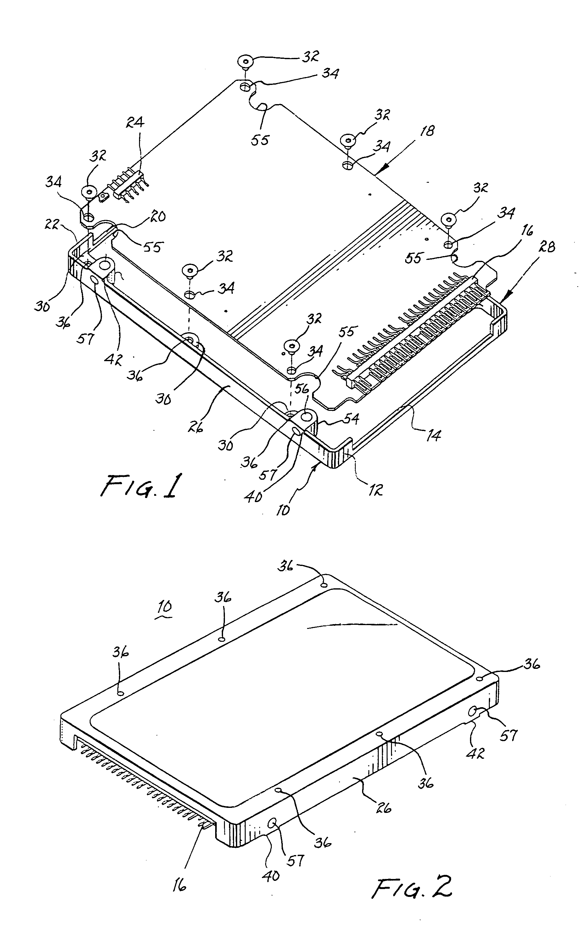
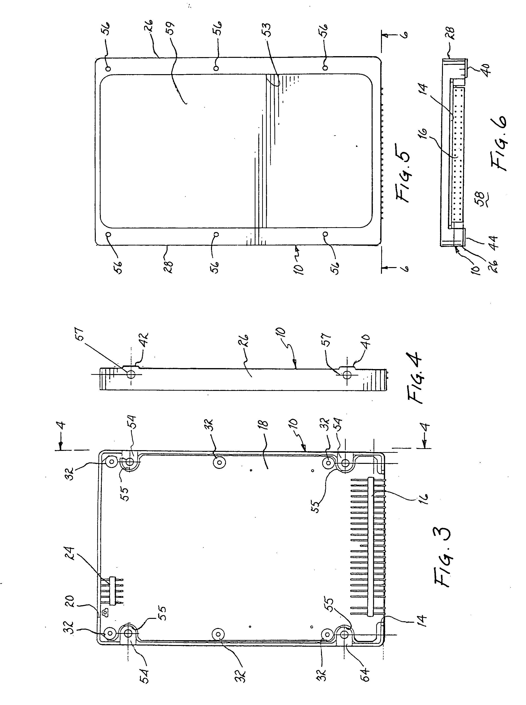
[0007] A cover, which forms a case for a single printed circuit board (PCB) has at least one partly cutaway sidewall and the PCB includes one or more electrical connectors having pins accessible through the cutaway sidewall. The cover includes standard sized threaded apertures for attachment of the case to a support element. To house more

Problems solved by technology

Printed circuit boards (hereinafter “PCBs”) are relatively densely populated with the relevant components but they are relatively fragile and may be damaged by rough handling during installation and replacement.

Method used


Image

  • Case for stackable PCBs
  • Case for stackable PCBs
  • Case for stackable PCBs

Examples


case 61

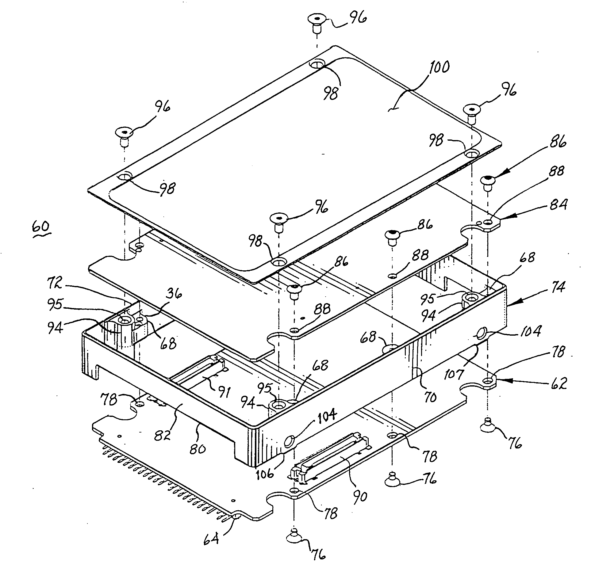
[0039] Case 61 may be attached to a support element by screws engaging the lower part of threaded passageway 95 in bosses 94. Spacer 74 includes further passageways 104 in sidewalls 70, 72 for use in attaching case 61 to a support element. Both of these modes of attachment are in accordance with the industry small form factor specification. Moreover, keys 106, 107 extend from sidewall 70 and similar keys, of which key 108 is shown in FIG. 9 and key 109 is shown in FIG. 16, extend from sidewall 72.

[0040] Referring jointly to FIGS. 10, 11 and 12, second variant 110 of a case 111 for stackable printed circuit boards (PCBs) will be described. As the second variant includes elements in addition to those described above with respect to first variant 60 (FIGS. 7, 8 and 9), common reference numerals will be used and the description of common elements will be relatively cursory. PCB 84 includes two or more electrical connectors 112, 113 extending upwardly therefrom. These electrical connecto...


PUM


Abstract

A case adapted for housing and protecting one or more stacked printed circuit boards and conforming with an industry small form factor specification. For a single printed circuit board, a cover includes sidewalls for encircling the printed circuit board and supports for attaching the printed circuit board thereto. The cover is keyed to and attached to a support element that may enclose the circuit board therewithin. One or more openings in the case provide access to external electrical connectors. For stacked printed circuit boards, a spacer supports a pair of printed circuit boards. A cover extends across the top of the spacer to enclose the printed circuit boards and screws extend through the cover into the spacer to secure these elements with one another. For additional printed circuit boards, further spacers, each supporting a printed circuit board are stacked between the first spacer and the cover.

Description

BACKGROUND OF THE INVENTION [0001] 1. Field of the Invention [0002] The present invention relates to modular units for enclosing printed circuit boards, and, more particularly, to a case for enclosing stacked printed circuit boards. [0003] 2. Description of Related Prior Art [0004] In the field of electronic equipment of various types, certain industry standards have been developed by the Electronic Industries Association (EIA) for the width and length of modular units housing various electronic equipment. Such standards may be referred to as form factor. In particular, these are EIA Specifications for Small Form Factor 63.5 mm (2.5″) disk drives and for Small Form Factor 88.9 mm (3.5″) disk drives. [0005] Printed circuit boards (hereinafter “PCBs”) are relatively densely populated with the relevant components but they are relatively fragile and may be damaged by rough handling during installation and replacement. Moreover, two or more PCBs may be required to satisfy the function an...

Claims


Application Information

Patent Timeline
IPC IPC(8): H05K7/14
CPCH05K7/1417
Inventor HAAGER, JAMES A.TUPA, RONALD E.FOGELSON, DANIEL P.
Owner ADTRON
Learn More