
Fabricating integrated devices using embedded masks

a technology of masks and integrated devices, applied in the field of integrated devices, can solve problems such as excessive local stresses, and achieve the effect of reducing the number of masks and masks

Active Publication Date: 2006-10-12
LUCENT TECH INC
View PDF15 Cites 14 Cited by
  • Summary
  • Abstract
  • Description
  • Claims
  • Application Information

AI Technical Summary

Benefits of technology

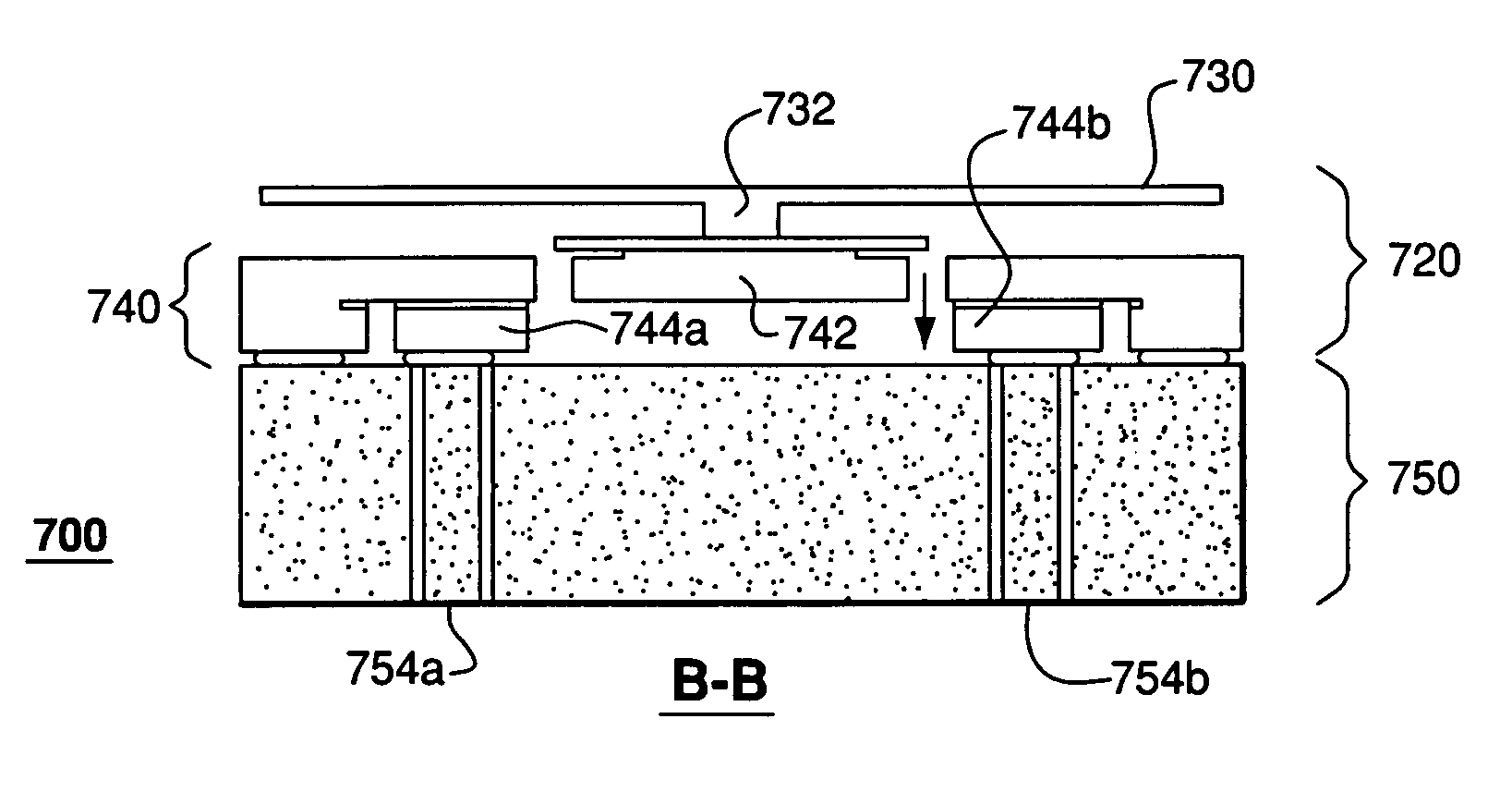
[0006] Problems in the prior art are addressed, in accordance with the principles of the present invention, by a method of fabricating a device using a multi-layered wafer that has an embedded etch mask adapted to map a desired device structure onto an adjacent (poly)silicon layer. Due to the presence of the embedded mask, it becomes possible to delay the etching that forms the mapped structure in the (poly)silicon layer until a relatively late fabrication stage. As a result, flatness of the (poly)silicon layer is preserved for the deposition of any necessary over-layers, which substantially obviates the need for filling the voids created by the structure formation with silicon oxide.

Problems solved by technology

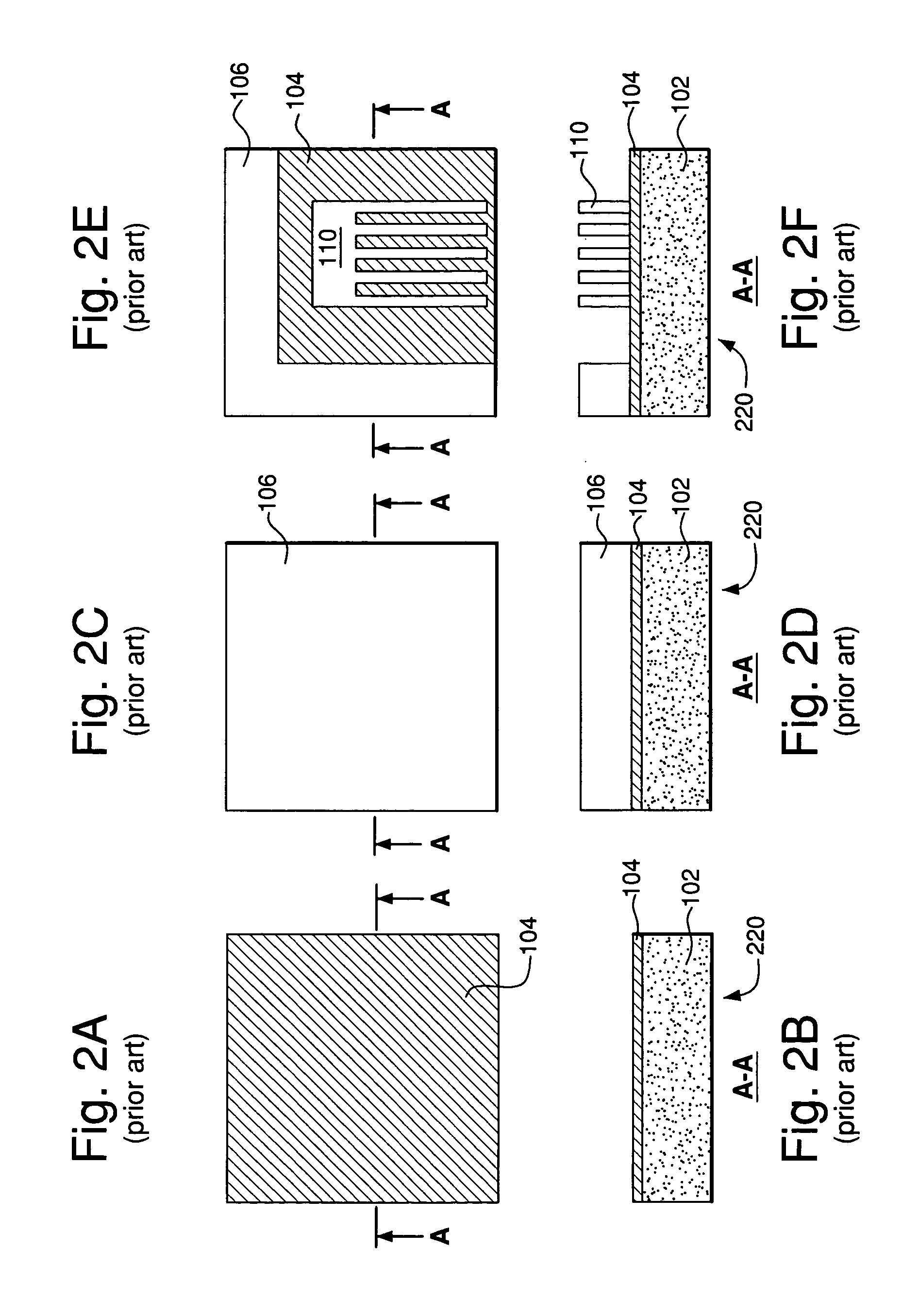
One significant difficulty associated with the oxide-filling step (i.e., step (2)) is that it often requires multiple deposition, etch-back, annealing, and polishing steps to achieve uniform filling of the voids and appropriate control of local stresses in nascent silicon structures (often having sub-micron dimensions).
Excessive local stresses are detrimental because these stresses can lead to fractures, e.g., during the final release procedure, when sacrificial silicon oxide is removed and substantial stresses might occur.

Method used


Image

  • Fabricating integrated devices using embedded masks
  • Fabricating integrated devices using embedded masks
  • Fabricating integrated devices using embedded masks

Examples


Embodiment Construction

[0018] Reference herein to “one embodiment” or “an embodiment” means that a particular feature, structure, or characteristic described in connection with the embodiment can be included in at least one embodiment of the invention. The appearances of the phrase “in one embodiment” in various places in the specification are not necessarily all referring to the same embodiment, nor are separate or alternative embodiments mutually exclusive of other embodiments.

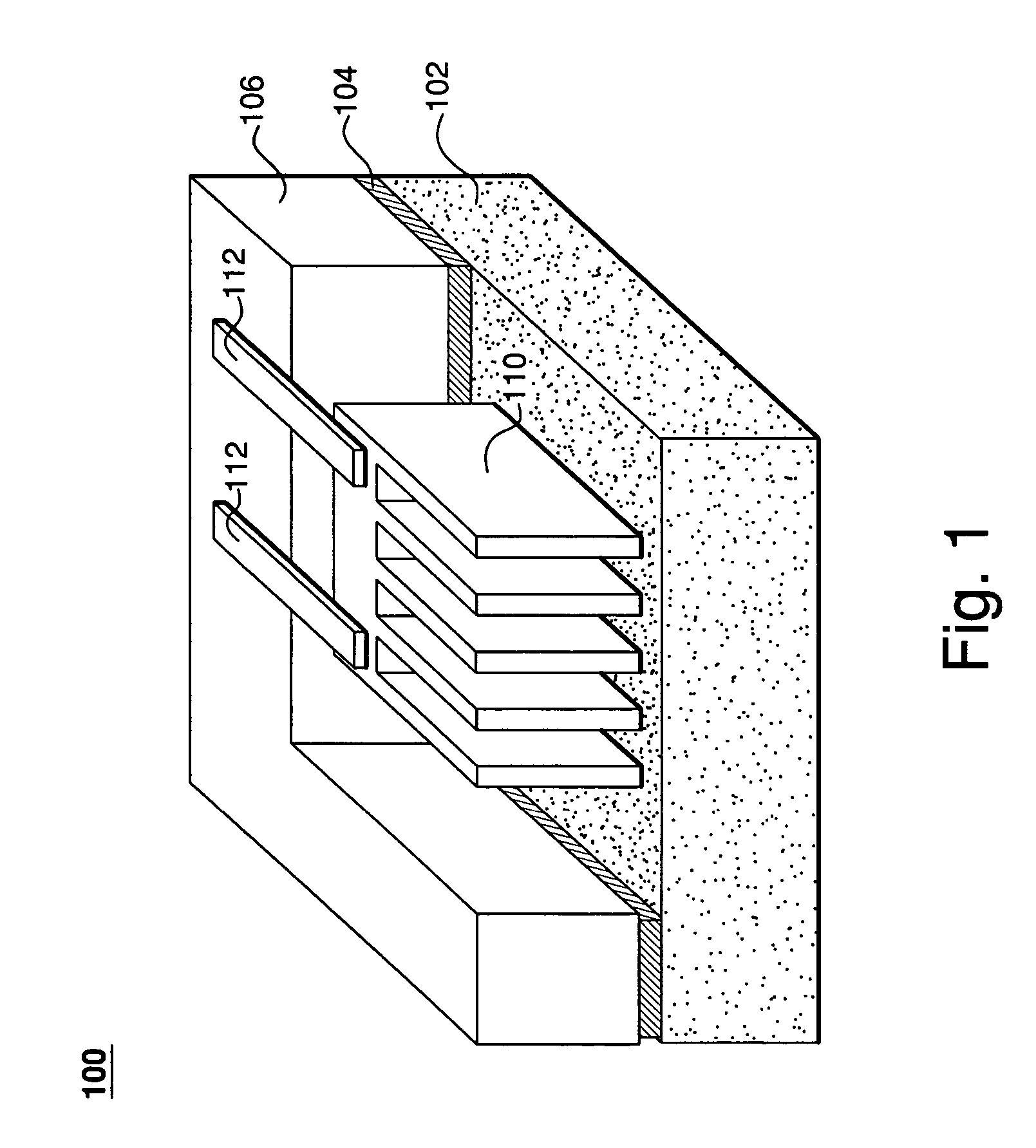
[0019]FIG. 1 shows a perspective three-dimensional view of a representative MEMS structure 100. More specifically, MEMS structure 100 includes a silicon substrate layer 102, a relatively thin silicon-oxide layer 104 deposited over the substrate layer, and a relatively thick (poly)silicon layer 106 deposited over the oxide layer. MEMS structure 100 further includes a comb-shaped electrode 110 movably connected to layer 106 by a pair of flexible bars (springs) 112. Electrode 110 can, for example, be a part of an electrostatic comb-...


PUM


Abstract

A method of fabricating a device using a multi-layered wafer that has an embedded etch mask adapted to map a desired device structure onto an adjacent (poly)silicon layer. Due to the presence of the embedded mask, it becomes possible to delay the etching that forms the mapped structure in the (poly)silicon layer until a relatively late fabrication stage. As a result, flatness of the (poly)silicon layer is preserved for the deposition of any necessary over-layers, which substantially obviates the need for filling the voids created by the structure formation with silicon oxide.

Description

[0001] The U.S. Government has a paid-up license in this invention and the right in limited circumstances to require the patent owner to license others on reasonable terms as provided for the terms of Contract No HR0011-04-C-0048 awarded by Coherent Communications Imaging and Targeting—Defense Advanced Research Projects Agency (CCIT-DARPA).BACKGROUND OF THE INVENTION [0002] 1. Field of the Invention [0003] The present invention relates to integrated devices and, more specifically, to methods for fabricating micro-electromechanical systems (MEMS) structures and / or devices. [0004] 2. Description of the Related Art [0005] Fabrication of a MEMS device often involves forming structures in one or more relatively thick (e.g., about 10 μm or thicker) layers of (poly)silicon. A typical prior-art method of forming such structures usually includes a sequence of: (1) patterning and etching a thick (poly)silicon layer down to an underlying silicon-oxide, etch-stop layer, which etching produces v...

Claims


Application Information

Patent Timeline
IPC IPC(8): H01L21/302H01L21/461
CPCB81C1/00404B81B2201/033
Inventor GREYWALL, DENNIS S.
Owner LUCENT TECH INC
Learn More