Sensor device
- Summary
- Abstract
- Description
- Claims
- Application Information
AI Technical Summary
Benefits of technology
Problems solved by technology
Method used
Image
Examples
example 1
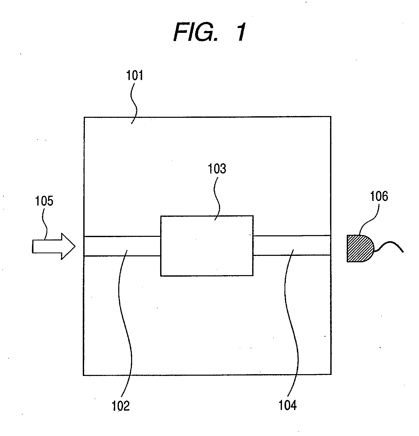
[0049] Two photonic crystals different in a property are optically connected serially, and sensing is conducted by utilizing transmitted light having transmitted through the two photonic crystals. The entire constitution of the sensor device of this Example is explained by reference to FIG. 1.
[0050] In FIG. 1, on substrate 101, photonic-crystal optical element system 103 is placed between light-introduction-side optical waveguide 102 and output-side optical waveguide 104. Incident light 105 is introduced from the outside of the element for measurement of the spectral transmittance of the photonic crystal optical element system. Optical detector device 106 detects the light having transmitted through optical waveguide 102, photonic crystal optical element system 103, and optical waveguide 104.
[0051] The photonic crystal optical element system in combination with a micro flow channel mentioned below will change its spectral transmissivity in accordance with an environmental change c...
example 2
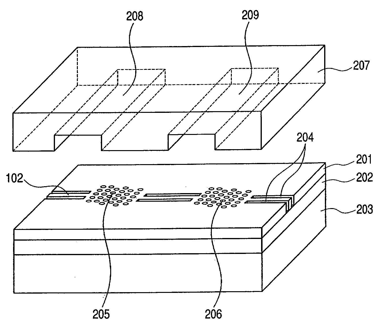
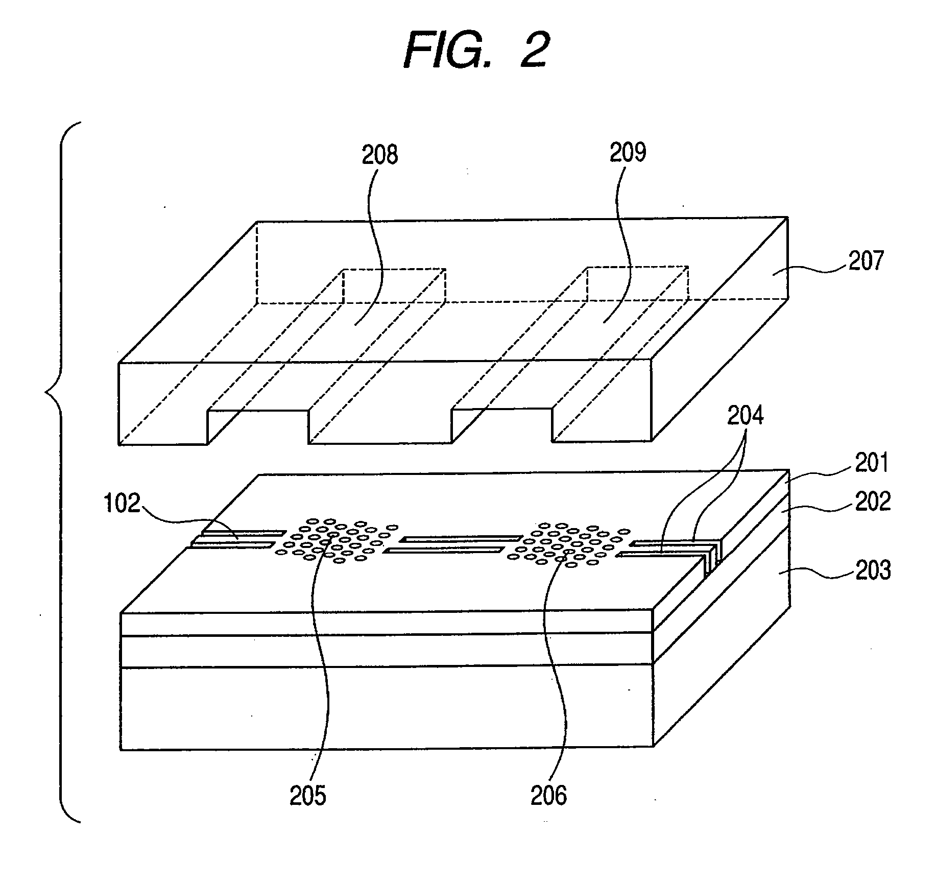
[0067] In this Example, two defect-containing photonic crystals having the same properties are optically connected in series, and sensing is conducted the utilizing transmitted light having transmitted through the two photonic crystals. The sensor device of this Example has a constitution similar to that shown in FIG. 1 as a whole. The photonic crystal element system is also similar to that in Example 1, and is shown in FIGS. 5A-5C. This example is different from Example 1 in first photonic crystal 205, second photonic crystal 206, and the incident light 105 for the detection.
[0068] In this Example, the two same photonic crystals are employed which have respectively a deficiency of a cylindrical hole and a defect-resonator 501. Thereby, the spectral transmittance of the photonic crystal has a sharp transmission peak corresponding to the defect level in the photonic band gap.
[0069] A sensing process by the sensor element constituted of the aforementioned micro flow channel element ...
example 3
[0079] In this Example, two photonic crystals having the same properties are optically connected in series, and the sensing is conducted the utilizing the light transmitted through a first photonic crystal region and then reflected by the second photonic crystal region.
[0080] Optical Waveguide
[0081] The sensor device of this Example has a constitution similar to that shown in FIG. 1 as a whole. FIG. 7 shows the constitution in more detail. In FIG. 7, first photonic crystal 205 and second photonic crystal 206 have the same properties, but the light is transmitted through the first photonic crystal and is reflected by the second photonic crystal, being different from the above Examples 1 and 2. For the optical connection of the transmitted light and the reflected light, Y-shaped coupling portion 703 is provided which is branched from optical guide 701 for the transmitted light into optical guides 705 for the light to be reflected. Thereby, transmitted light 702 is introduced to the ...
PUM
 Abstract
Description
Claims
Application Information
 - R&D
- Intellectual Property
- Life Sciences
- Materials
- Tech Scout
- Unparalleled Data Quality
- Higher Quality Content
- 60% Fewer Hallucinations
Browse by: Latest US Patents, China's latest patents, Technical Efficacy Thesaurus, Application Domain, Technology Topic, Popular Technical Reports.
© 2025 PatSnap. All rights reserved.Legal|Privacy policy|Modern Slavery Act Transparency Statement|Sitemap|About US| Contact US: help@patsnap.com


