
Processes for planarizing substrates and encapsulating printable electronic features

a technology of electronic features and substrates, applied in the field of printing electronic features, can solve the problems of low viscosity compositions not being developed as well as high viscosity compositions, substrate variability, and substrates often showing high irregular surfaces

Inactive Publication Date: 2006-07-20
CABOT CORP
View PDF99 Cites 54 Cited by
  • Summary
  • Abstract
  • Description
  • Claims
  • Application Information

AI Technical Summary

Benefits of technology

[0009] The present invention is directed processes for planarizing substrate, encapsulating electronic features and forming ramping features on substrates. In one embodiment, for example, the invention is to a process for forming an electronic feature on a second substrate, the process comprising the steps of: (a) providing a first substrate having a first surface, wherein the first surface has a surface irregularity; (b) applying a planarizing agent to at least a portion of ...

Problems solved by technology

However, low viscosity compositions are not as well developed as the high viscosity compositions.
One problem associated with the formation of printable electronic features is substrate variability.
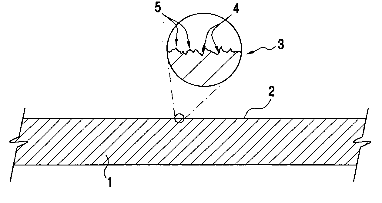
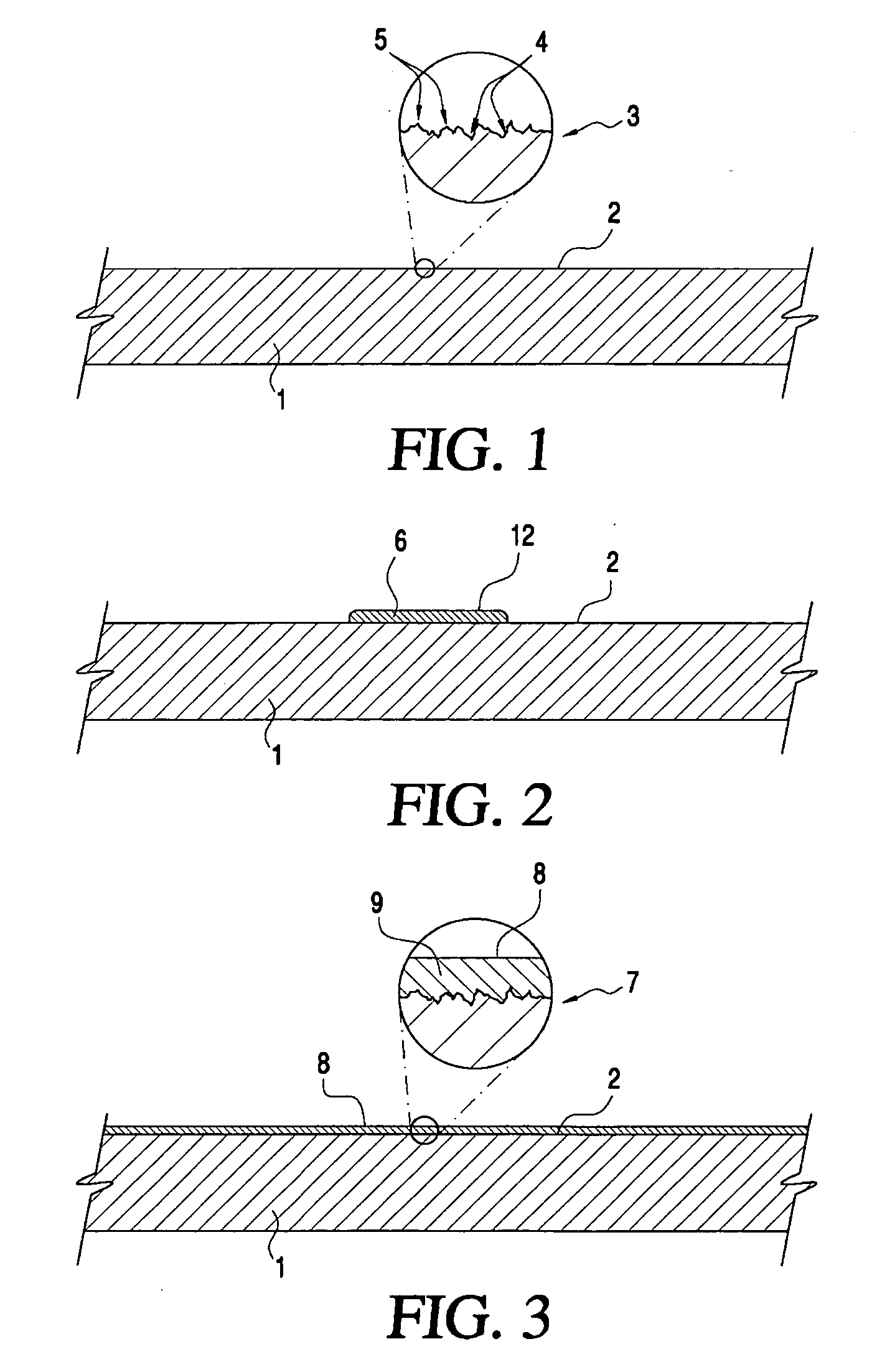
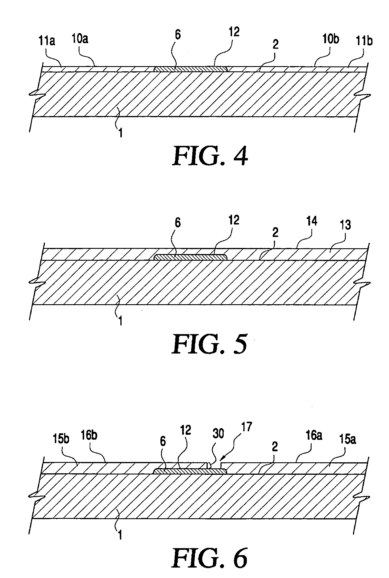
Although most substrates typically provide, at a macroscopic level, a substantially planar surface for receiving a printable electronic feature, such substrates often exhibit highly irregular surfaces on a microscopic level.
These surface irregularities may result in variability of the electronic properties of the printable electronic features ultimately formed thereon.
Accordingly, it may be difficult to repeatably form a printable electronic feature having desired electronic properties on an irregular substrate surface.
Another problem associated with electronic features formed by direct write (e.g., ink-jet) printing techniques is that they may exhibit circuit instability and variation due to atmospheric exposure.
Similarly, water in the air may slowly react with the components in the electronic features, particularly resistive compositions contained in certain electronic features, to cause an undesired change in electrical properties.

Method used


Image

  • Processes for planarizing substrates and encapsulating printable electronic features
  • Processes for planarizing substrates and encapsulating printable electronic features
  • Processes for planarizing substrates and encapsulating printable electronic features

Examples


Embodiment Construction

[0039] I. Introduction

[0040] In one aspect, the present invention is directed to processes for planarizing a substrate prior to application of an electronic ink to form a printed electronic feature. As used herein, the term “planarizing” and variations thereof means modifying a substrate surface to make it more planar (e.g., on a microscopic and / or on a macroscopic scale). In one aspect, for example, the process comprises the steps of: (a) providing a first substrate having a first surface, wherein the first surface has a surface irregularity; (b) applying a planarizing agent to at least a portion of the first surface; (c) treating the applied planarizing agent under conditions effective to form the second substrate, the second substrate comprising the first substrate and a planarizing feature formed from the planarizing agent, wherein the second substrate has a planar surface formed at least in part of the planarizing feature, the planar surface being more planar than the first su...


PUM

PropertyMeasurementUnit
Temperatureaaaaaaaaaa
Viscosityaaaaaaaaaa
Surface tensionaaaaaaaaaa

Abstract

Processes for planarizing a substrate, for encapsulating a printed electronic feature and for forming a ramp feature. In various embodiments, the processes include the steps of: (a) applying a planarizing agent, an encapsulating agent or a ramping feature to a substrate or to an electronic feature disposed thereon, preferably through a direct write printing process, e.g., ink-jet printing, and (b) treating the applied agent under conditions effective to form a planarizing feature, an encapsulation layer or a ramping feature.

Description

CROSS REFERENCE TO RELATED APPLICATIONS [0001] This patent application claims priority to U.S. Provisional Patent Application Ser. Nos. 60 / 643,577; 60 / 643,629; and 60 / 643,378, all filed on Jan. 14, 2005, and to U.S. Provisional Patent Application Ser. No. 60 / 695,412, filed on Jul. 1, 2005, the entireties of which are all incorporated herein by reference.FIELD OF THE INVENTION [0002] The present invention relates to printing electronic features. More specifically, the invention relates to planarization and encapsulation techniques that may be used during the formation of printable electronic features. BACKGROUND OF THE INVENTION [0003] The electronics, display and energy industries rely on the formation of coatings and patterns of conductive materials on substrates to form circuits on organic and inorganic substrates. The primary methods for generating these patterns are screen printing for features larger than about 100 μm and thin film and etching methods for features smaller than ...

Claims


Application Information

Patent Timeline
IPC IPC(8): H01L21/31H01L21/469
CPCH01L21/31053H01L51/0005H01L2224/24998H01L2224/76155H01L2924/09701H05K1/095H05K1/097H05K1/16H05K3/1208H05K3/125H05K3/386H05K3/389H05K3/4667H05K2201/09836H05K2201/09909H05K2203/013H05K2203/0594H01L2924/01019H01L2224/82007H10K71/135
Inventor KOWALSKI, MARK H.VANHEUSDEN, KARELEDWARDS, CHUCK
Owner CABOT CORP
Learn More