Semiconductor light emitting device
- Summary
- Abstract
- Description
- Claims
- Application Information
AI Technical Summary
Benefits of technology
Problems solved by technology
Method used
Image

Examples
first embodiment
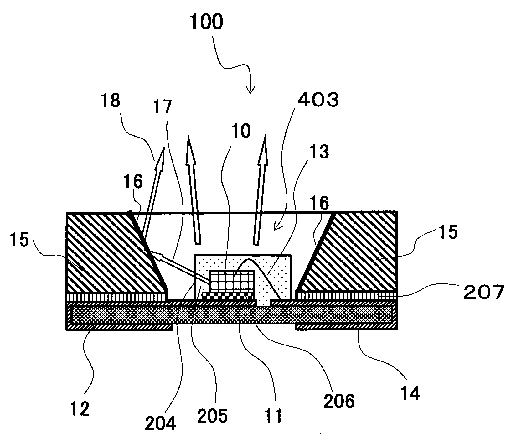
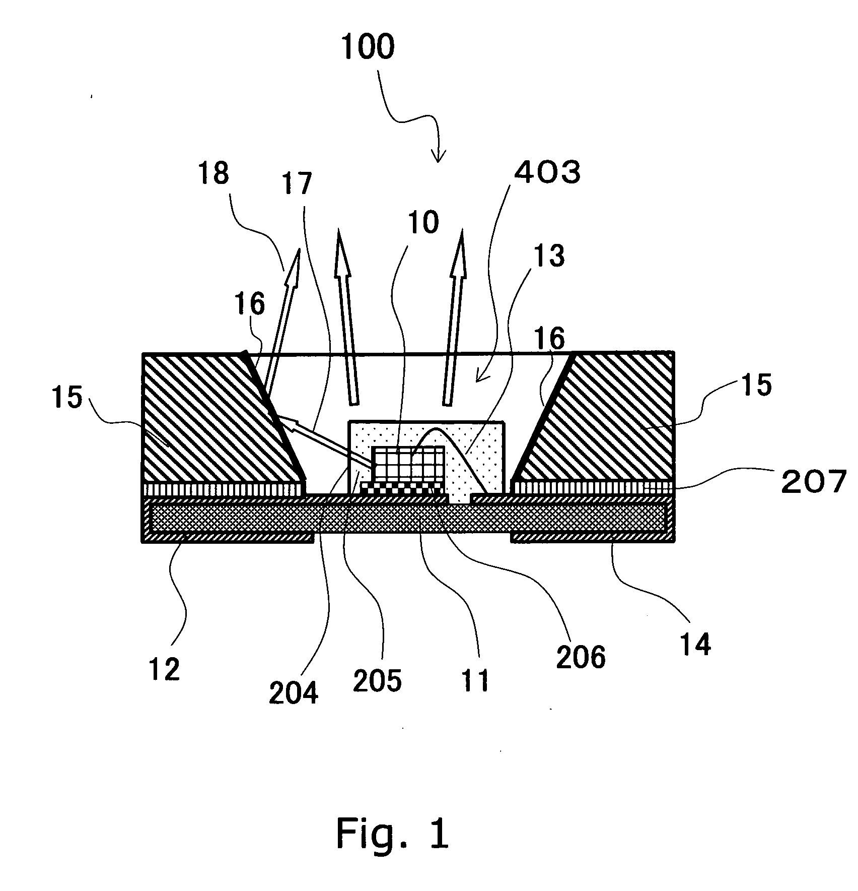
[0036]FIG. 1 is a schematic cross sectional view of a semiconductor light emitting device in accordance with a first embodiment of the present invention. A semiconductor light emitting device 100 is shown in FIG. 1.
[0037] A semiconductor light emitting element 10 (abbreviated LED chip 10) is configured to emit ultra violet light or longer wavelength light. The LED chip 10 is mounted on a first electrode pattern 12 of an insulating substrate 11 with an AuSn eutectic solder 206. The melting point of the AuSn eutectic solder 206 is about 280 Centigrade. An electrode, which is provided on a top surface of the LED chip 10, and a second electrode pattern 14 are electrically connected by a wire 13. The LED chip 10 and the wire 13 are sealed by a resin 204. The substrate 11 may be AlN, which has a good heat releasing. A ceramic, an Al2O3, or a printed circuit board which a heat extraction member is pressed in the substrate 11.
[0038] The LED chip 10 may be a chip provided on an insulating ...
second embodiment
[0108] A second embodiment of the present invention will be explained hereinafter with reference to FIG. 17. FIG. 17 is a schematic cross sectional view of a semiconductor light emitting device in accordance with the second embodiment.
[0109] A semiconductor light emitting device 103 is described in accordance with this second embodiment of the present invention. With respect to each portion of this embodiment, the same or corresponding portions of the semiconductor light emitting device of the first embodiment or its modified embodiment as shown in FIGS. 1-16 are designated by the same reference numerals, and its explanation of such portions is omitted.
[0110] The metal body 15 may be charged during a manufacturing process. Generally the light emitting element (LED chip) has smaller ESD resistance than the silicon device.
[0111] In this second embodiment, the metal body 15 is electrically connected via a bump 73 with one of the first electrode 12 and the second electrode 14 of the ...
third embodiment
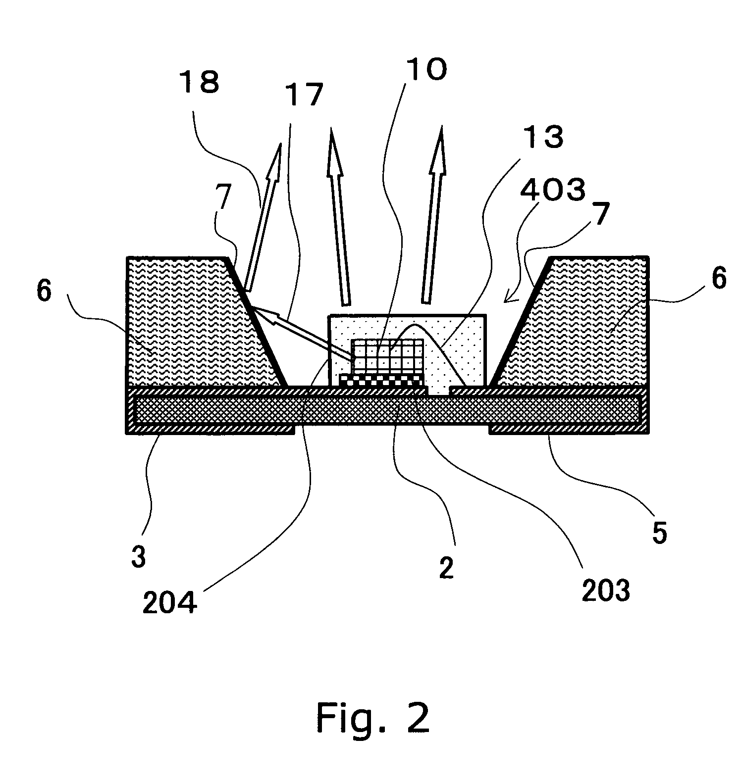
[0115] A third embodiment of the present invention will be explained hereinafter with reference to FIG. 18. FIG. 18 is a schematic cross sectional view of a semiconductor light emitting device in accordance with the third embodiment.
[0116] A semiconductor light emitting device 104 is described in accordance with this third embodiment of the present invention. With respect to each portion of this embodiment, the same or corresponding portions of the semiconductor light emitting device of the first, second embodiment or its modified embodiment as shown in FIGS. 1-17 are designated by the same reference numerals, and its explanation of such portions is omitted.
[0117] In this embodiment, a print circuit board 2 is used as the insulating substrate 11 instead of ceramic board. An electrode 3, 5 are provided on both sides (upper and lower side) of the print circuit board 2. A heat extraction member 64 can be provided in a center portion of the print circuit board 2. The LED chip 10 can b...
PUM
 Abstract
Description
Claims
Application Information
 - R&D
- Intellectual Property
- Life Sciences
- Materials
- Tech Scout
- Unparalleled Data Quality
- Higher Quality Content
- 60% Fewer Hallucinations
Browse by: Latest US Patents, China's latest patents, Technical Efficacy Thesaurus, Application Domain, Technology Topic, Popular Technical Reports.
© 2025 PatSnap. All rights reserved.Legal|Privacy policy|Modern Slavery Act Transparency Statement|Sitemap|About US| Contact US: help@patsnap.com