
Data latch

a data latch and latch technology, applied in the field of data latches, can solve the problems of overcompensating the slow response speed of the latch, and achieve the effect of reducing the settling time and the chip area of the latch

Active Publication Date: 2006-05-18
REALTEK SEMICON CORP
View PDF3 Cites 10 Cited by
  • Summary
  • Abstract
  • Description
  • Claims
  • Application Information

AI Technical Summary

Benefits of technology

[0008] According to the claimed invention, a high-speed latch is disclosed. The latch includes a latch unit comprising a first input terminal for receiving a first input signal and a first output terminal for outputting a first output signal; and a first current source coupled to the first output terminal, the first current source being enabled for providing the first output terminal with a first driving current to reduce a voltage difference between the first output signal and the first input signal when the first output signal and the first input signal correspond to different logic states.
[0011] It is an advantage of the claimed invention that the current sources can provide an auxiliary driving current so as to reduce the settling time and chip area of the latch.

Problems solved by technology

However, as a result of the ever-increasing operating speeds of digital circuits, one important issue is to overcome the slow response speed of the latch.

Method used


Image

  • Data latch
  • Data latch
  • Data latch

Examples


Embodiment Construction

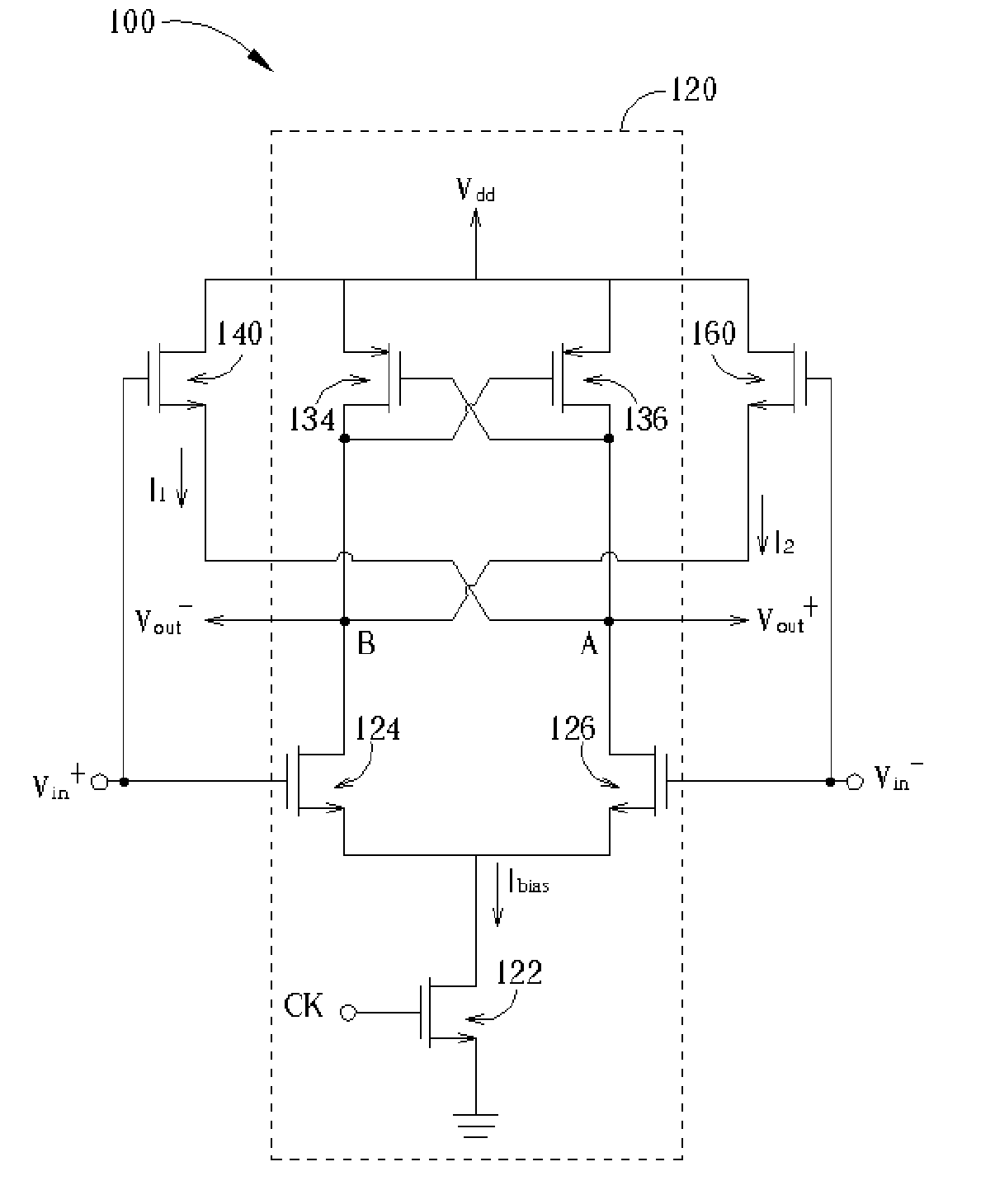
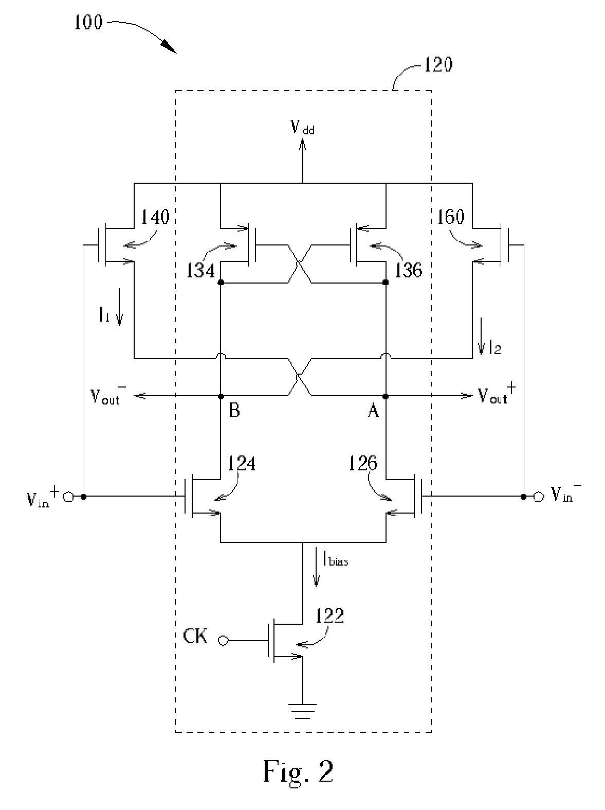
[0016] Please refer to FIG. 2, which is a schematic diagram of a high-speed latch 100 according to the present invention. As shown, the latch 100 includes a latch unit 120 and two current sources 140, 160. The latch unit 120 has differential output terminals A, B. In an embodiment, the latch unit 120 is composed of NMOS transistors 122, 124, 126 and PMOS transistors 134, 136. The NMOS transistor 122 is used to provide a bias current Ibias for the NMOS transistors 124 and 126 when the clock signal CK is logic high. That is, if the NMOS transistor 122 is enabled (turned on), the bias current Ibias is induced. It is clear that only when the clock signal CK is logic high, the latch unit 120 is active and able to drive the differential output signals Vout+, Vout− according to the differential input signals Vin+, Vin−. The related operation is further detailed in the flowing description.

[0017] As shown in FIG. 2, the NMOS transistors 124, 126 act as a differential pair to receive the dif...


PUM


Abstract

A high-speed latch includes a latch unit and a first current source. The latch unit has a first input terminal for receiving a first input signal and a first output terminal for outputting a first output signal. The first current source is coupled to the first output terminal, and is enabled for providing the first output terminal with a first driving current to reduce a voltage difference between the first output signal and the first input signal when the first output signal and the first input signal correspond to different logic states.

Description

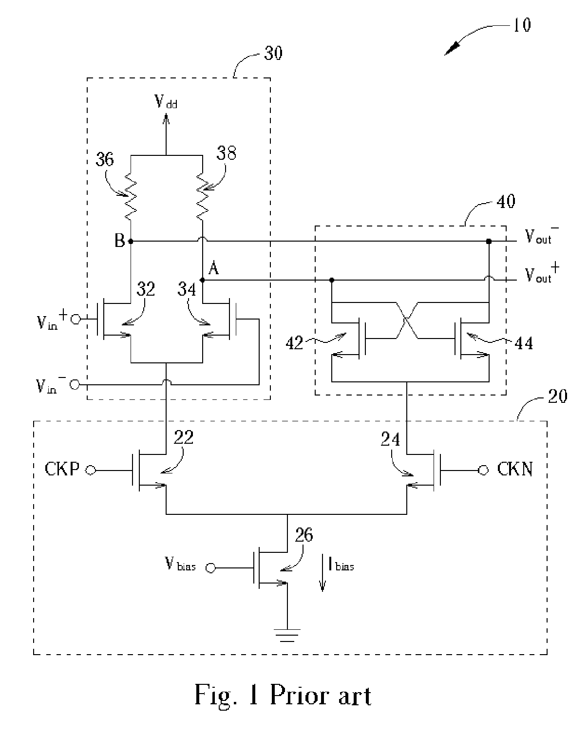
BACKGROUND OF INVENTION [0001] 1. Field of the Invention [0002] The invention relates to a data latch, and more particularly, to a high-speed data latch. [0003] 2. Description of the Prior Art [0004] A data latch is a common device used in digital circuits for latching an input signal. For instance, a conventional flip-flop composed of two latches is often used for implementing a frequency divider in a digital circuit. However, as a result of the ever-increasing operating speeds of digital circuits, one important issue is to overcome the slow response speed of the latch. Please refer to FIG. 1 showing a schematic diagram of high-speed latch 10 implemented using NMOS transistors according to the prior art. As shown in FIG. 1, the high-speed latch 10 includes a clocked current source 20, a differential amplifier 30, and a latch unit 40. The clocked current source 20 includes three NMOS transistors 22, 24, 26. The NMOS transistors 22 and 24 are enabled (turned on) by the clock signals ...

Claims


Application Information

Patent Timeline
Patent Type & Authority Applications(United States)
IPC IPC(8): G11C7/10
CPCH03K3/012H03K3/356104
Inventor RAZAVI, BEHZADKANG, HAN-CHANG
Owner REALTEK SEMICON CORP
Learn More