Negative-resistance circuit and active filter
a negative resistance and active filter technology, applied in the field of negative resistance circuits and active filters, can solve the problems of large fluctuations in filter characteristics, difficult adjustment, and difficulty in achieving constant negative resistance values
- Summary
- Abstract
- Description
- Claims
- Application Information
AI Technical Summary
Benefits of technology
Problems solved by technology
Method used
Image

Examples
first embodiment
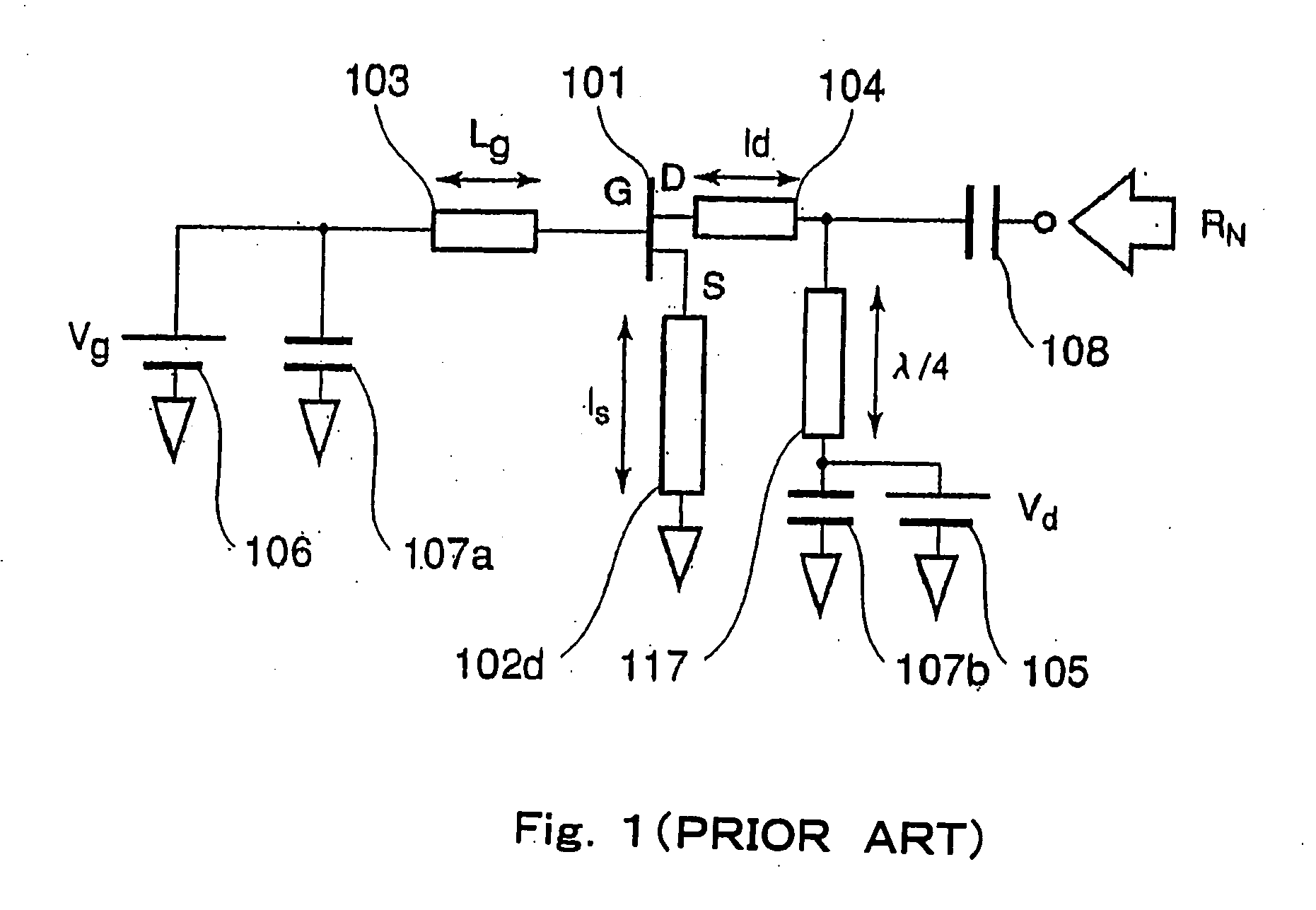
[0046] A negative-resistance circuit according to a first embodiment of the present invention comprises field effect transistor (FET) 1, as illustrated in FIG. 4, and is configured to have negative resistance RN by positively feeding back from drain (D) to gate (G) of FET 1. Connected to a source of FET 1 is first distributed constant line (the length of which is ls1) which is capacitive in a desired frequency range, grounds the source in a direct current manner, and has a length set in a range λ / 4<ls<λ / 2 (λ is one wavelength at a desired frequency).
[0047] Capacitance element 7a is connected to drain (D) of FET 1 through second distributed constant line (the length of which is ld) 3 for short-circuiting to a ground potential in a high frequency manner. Also, the drain of FET 1 is applied with predetermined bias voltage Vd by bias power source 5 through second distributed constant line 3.
[0048] Third distributed constant line (the length of which is lg) 4 is connected to the gate o...
second embodiment
[0062] As illustrated in FIG. 11, a negative-resistance circuit according to a second embodiment comprises fourth distributed constant line 2b (the length of which is ls2) connected to source (S) of an FET in parallel with first distributed constant line 2a (the length of which is ls1) shown in FIG. 4 (where ls1>ls2). Since the remaining configuration is similar to the first embodiment, description thereon is omitted.
[0063] In the negative-resistance circuit of the second embodiment illustrated in FIG. 11, the phase of a reflection coefficient of first distributed constant line 2a and fourth distributed constant line 2b changes with respect to the frequency in a non-linear fashion, as viewed from the source of the FET. FIG. 12 is a graph showing this situation. FIG. 12 shows the phase characteristics with respect to a change in frequency when length ls2 of fourth distributed constant line 2b is changed under the condition of ls1>ls2, with first distributed constant line 2a having l...
third embodiment
[0069] As illustrated in FIG. 14, a negative-resistance circuit according to a third embodiment comprises fifth distributed constant line 2c (the length of which is ls3) which is set to a length equal to or shorter than one-quarter wavelength at a desired frequency and has an opened leading end, and sixth distributed constant line 2d (the length of which is ls4) having a leading end connected to the ground potential, both of which are connected to the source of the FET. Since the remaining configuration is similar to the first embodiment, description thereon is omitted.
[0070] Likewise, in such a configuration, the phase of reflection coefficient of fifth distributed constant line 2c and sixth distributed constant line 2d changes non-linearly with respect to the frequency, as viewed from the source of the FET, as shown in FIG. 15. Accordingly, the negative-resistance circuit of the third embodiment can provide similar effects to those in the second embodiment.
[0071] While the secon...
PUM
 Abstract
Description
Claims
Application Information
 - R&D
- Intellectual Property
- Life Sciences
- Materials
- Tech Scout
- Unparalleled Data Quality
- Higher Quality Content
- 60% Fewer Hallucinations
Browse by: Latest US Patents, China's latest patents, Technical Efficacy Thesaurus, Application Domain, Technology Topic, Popular Technical Reports.
© 2025 PatSnap. All rights reserved.Legal|Privacy policy|Modern Slavery Act Transparency Statement|Sitemap|About US| Contact US: help@patsnap.com