Chip card module

a chip card module and chip card technology, applied in the field of chip card modules, can solve the problems of misuse, inability to detect misuse, and difficulty in the case of contactless chip cards,

Inactive Publication Date: 2006-03-02
INFINEON TECH AG
View PDF27 Cites 9 Cited by
  • Summary
  • Abstract
  • Description
  • Claims
  • Application Information

AI Technical Summary

Problems solved by technology

While in the case of chip cards with contacts it is possible at least in the case of some applications for a check to be carried out on the persons using them, for example by keeping an ATM under video surveillance, it is more difficult in the case of contactless chip cards, since they sometimes even operate from relatively great distances.
Moreover, in the case of contactless chip cards, there is no optical checking of the card, so that misuse cannot be detected and prevented by optical scanning of security features on the chip card.
A disadvantage of this known method is that, for it to be applied in the case of contactless chip cards, the chip card must in turn be brought into direct contact with the read / write unit, in order that a detector can pick up the foreign particle information.

Method used


Image

  • Chip card module
  • Chip card module
  • Chip card module

Examples


Embodiment Construction

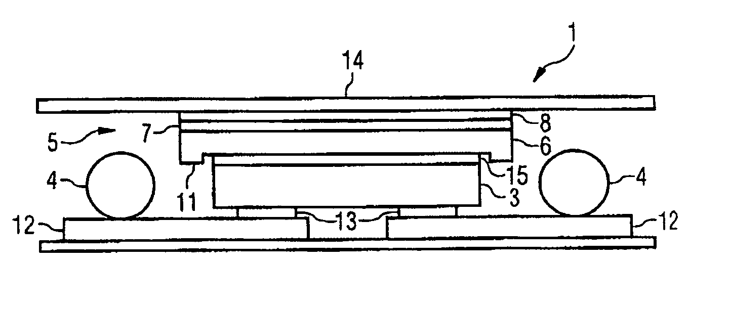
[0018] The present invention is directed to a chip card module wherein a layer sequence is formed on a surface side of the chip card module, with a first layer, reflecting electromagnetic waves, a second layer, arranged on this first layer, and a third layer, in which a metallic cluster is embedded, arranged on the second layer.

[0019] A first advantage of the chip card module according to the invention for contactless chip cards is that the layer sequence produces an individual marking, which is independent of the card in which a chip card module is received. This prevents a forged chip card module being inserted in the “genuine” card. The planned misuse of chip cards can be discovered already when chip card modules are brought into circulation, so that countermeasures can be taken at an early stage. Use of the chip card module forgery cannot be concealed by subsequent manipulations of a card body in which the forged chip card modules are inserted.

[0020] The use according to the i...


PUM


Abstract

A chip card module for a contactless chip card having a chip containing an integrated circuit, and having a coupling element, electrically connected to the chip to permit contactless communication. The chip card module has a layer sequence formed on a surface side of the chip card module, with a first layer reflecting electromagnetic waves, a second layer arranged on this first layer, and a third layer, in which a metallic cluster is embedded, arranged on the second layer.

Description

CROSS-REFERENCE TO RELATED APPLICATION [0001] This application claims priority to German Patent Application Serial No. 102004042187.0, which was filed Aug. 31, 2004 and is incorporated herein by reference in its entirety. FIELD OF THE INVENTION [0002] The invention relates to a chip card module for a contactless chip card, having a chip, containing an integrated circuit, and having a coupling element, electrically connected to the chip to permit contactless communication. BACKGROUND OF THE INVENTION [0003] Chip cards have long been known and are increasingly used for example as phone cards, identity cards or the like. Contactless chip cards communicate with a read / write unit via an electromagnetic field. An electromagnetic field is in this case generated in the read / write unit, its modulation allowing data to be transferred to a chip card which is located in this field in adequate proximity to the read / write unit. For this purpose, the chip card is equipped with a coupling element, ...

Claims


Application Information

Patent Timeline
Patent Type & Authority Applications(United States)
IPC IPC(8): G06K19/06
CPCG06K19/07745G06K19/07747H01L2924/01079H01L2224/73253H01L2224/16H01L2924/00014H01L2924/00011H01L2224/0401
Inventor PUSCHNER, FRANKSTAMPKA, PETERMULLER-HIPPER, ANDREASSCHINDLER, WOLFGANG
Owner INFINEON TECH AG
Why Eureka
Try Eureka