
Semiconductor nanocrystal complexes and methods of making same

a technology of crystal complexes and semiconductors, applied in the direction of crystal growth process, natural mineral layered products, synthetic resin layered products, etc., can solve the problems of lattice mismatch between a core and a core, reducing quantum yield, and reducing fluorescence quantum yield over tim

Active Publication Date: 2006-01-19
SAMSUNG ELECTRONICS CO LTD
View PDF9 Cites 58 Cited by
  • Summary
  • Abstract
  • Description
  • Claims
  • Application Information

AI Technical Summary

Benefits of technology

The present invention provides a semiconductor nanocrystal complex that includes a semiconductor nanocrystal core with a metal layer formed on its outer surface after synthesis. The complex may also have a shell overcoating the metal layer, which is preferably made of a semiconductor material with a larger bulk bandgap than that of the nanocrystal core. The technical effect of this invention is to provide a more stable and efficient semiconductor nanocrystal complex with improved optical properties.

Problems solved by technology

Because the nanocrystal may have a large surface area to volume ratio, dislocations present on the surface or adsorbed surface molecules having a significant potential difference from the nanocrystal itself will tend to trap excited state carriers and prevent radiactive recombination and thus reduce quantum yield.
A problem associated with the above attempts at making semiconductor nanocrystals is a marked decrease in the fluorescence quantum yield over time due to oxidation of the nanocrystal.
An additional problem associated with attempts to synthesize semiconductor nanocrystal complexes is the presence of lattice mismatch between a core semiconductor layer and the semiconductor shell.
The presence of lattice mismatch reduces the quantum efficiency of a given semiconductor nanocrystal complex due to its effects on recombination.

Method used


Image

  • Semiconductor nanocrystal complexes and methods of making same
  • Semiconductor nanocrystal complexes and methods of making same
  • Semiconductor nanocrystal complexes and methods of making same

Examples


example

Preparing A Semiconductor Nanocrystal Complex

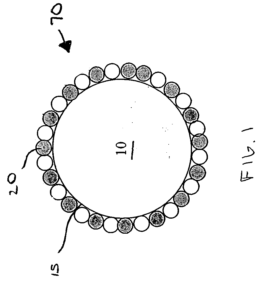
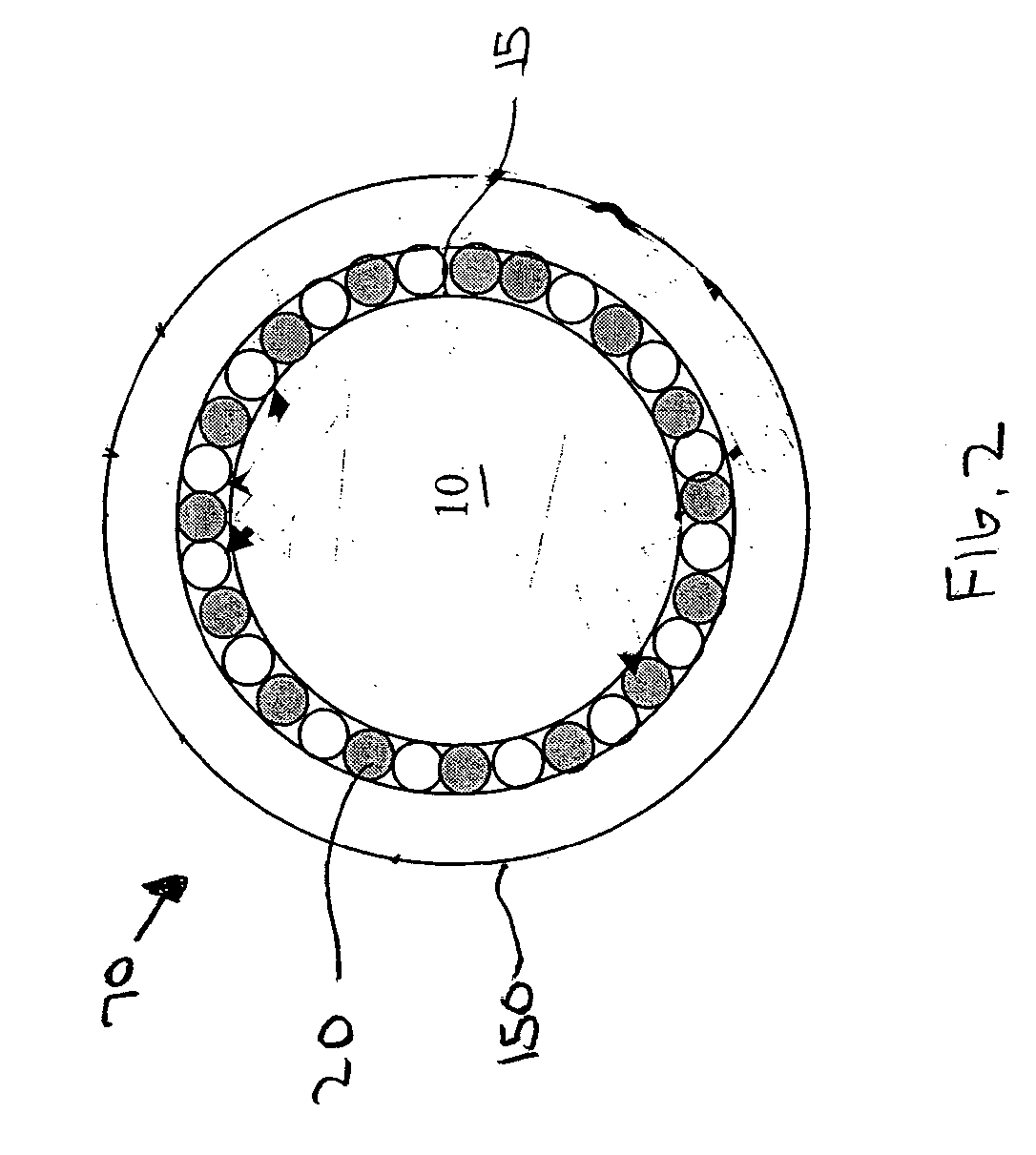
[0036] The present examples discloses how to make a semiconductor nanocrystal complex comprising a semiconductor nanocrystal core, a metal layer formed on the semiconductor nanocrystal core after synthesis of the semiconductor nanocrystal core and a semiconductor shell overcoating the metal layer.

[0037] 20 grams of technical grade TOPO was loaded into each of two 100 ml reaction flasks. After the flasks were purged for 5 minute by nitrogen, the reaction flasks were heated to 130° C. using heating mantles. The system was switched to a vacuum system to purify the solvent (technical grade TOPO). After 10 minutes at 130° C. purification, the temperature was increased to 190° C. for further purification for one to two hours. Next, the reaction flasks containing the purified TOPO was cooled down to 70° C. and filled with nitrogen. In reaction flask 1, one of the 100 ml reaction flasks, 2 ml purified CdTe core dots in toluene (30 mg / ml) was i...


PUM

PropertyMeasurementUnit
diameteraaaaaaaaaa
diameteraaaaaaaaaa
mean diameteraaaaaaaaaa

Abstract

A semiconductor nanocrystal complex including a metal layer formed on the outer surface of a semiconductor nanocrystal core after synthesis of the semiconductor nanocrystal core and a method for preparing a nanocrystal complex comprising forming a metal layer on a semiconductor nanocrystal core after synthesis of the semiconductor nanocrystal core. The metal layer may passivate the surface of the semiconductor nanocrystal core and protect the semiconductor nanocrystal core from the effects of oxidation. Also provided is a semiconductor nanocrystal complex with a shell grown onto the metal layer formed on the semiconductor nanocrystal core. In this embodiment, the metal layer may prevent lattice mismatch between the semiconductor shell and the semiconductor nanocrystal core.

Description

CROSS-REFERENCE TO RELATED APPLICATIONS [0001] The present application claims priority to U.S. Provisional Application No. 60 / 569,452, filed May 10, 2004, which is incorporated by reference herein.FIELD OF THE INVENTION [0002] The present invention relates to semiconductor nanocrystal complexes and particularly to semiconductor nanocrystal complexes having a metal layer formed on a semiconductor nanocrystal core. The present invention also relates to methods of making such semiconductor nanocrystal complexes. BACKGROUND OF THE INVENTION [0003] Semiconductor nanocrystals are typically tiny crystals of II-VI, III-V, IV-VI materials that have a diameter between 1 nanometer (nm) and 20 nm. In the strong confinement limit, the physical diameter of the nanocrystal is smaller than the bulk excitation Bohr radius causing quantum confinement effects to predominate. In this regime, the nanocrystal is a 0-dimensional system that has both quantized density and energy of electronic states where ...

Claims


Application Information

Patent Timeline
Patent Type & Authority Applications(United States)
IPC IPC(8): B32B9/04B32B15/00B05D1/36B05D7/00C01B19/00C30B7/00C30B29/60
CPCB82Y20/00Y10S977/821C01G9/08C01G11/02C01G13/00C01G21/21C01G25/00C01P2004/64C01P2006/40C09K11/02C09K11/025C09K11/565C09K11/62C09K11/661C09K11/70C09K11/7492C09K11/75C09K11/88C09K11/883C09K11/892C23C18/00C23C18/1204C23C18/1295C30B7/00C30B29/605C30B33/00B82Y30/00Y10S977/817Y10T428/12528Y10T428/2982Y10T428/12535Y10T428/2991Y10T428/1266Y10T428/12785Y10S977/773Y10S977/834Y10S977/774Y10S977/815Y10S977/813Y10S977/818Y10S977/819Y10S977/816Y10S977/82Y10S977/822Y10S977/823
Inventor PENG, ADAMLIU, WEI
Owner SAMSUNG ELECTRONICS CO LTD
Learn More