Selective light absorption shifting layer and process

a technology of selective light absorption and shifting layer, which is applied in the direction of semiconductor lasers, active medium materials, instruments, etc., can solve the problems of difficult to perform micron-scale patterning in a reproducible fashion on the laser structure, high power density cannot be obtained, and method has not been fully established, so as to achieve the effect of easing manufacturing

Inactive Publication Date: 2006-01-05
EASTMAN KODAK CO
View PDF9 Cites 11 Cited by
  • Summary
  • Abstract
  • Description
  • Claims
  • Application Information

AI Technical Summary

Benefits of technology

[0015] The invention also provides for forming an image or an information record and a composition of matter. The invention provides methods for forming filters, images or information records having a smooth surface and in particular for forming a pixel region pattern for use with an Organic VCSEL that would ease manufacturing.

Problems solved by technology

Such high power densities can only be obtained by using other lasers as the pump sources, precluding that route for inorganic laser cavities.
This result is highly significant for amorphous organic laser systems, since driving them by electrical injection has, to this date, been unobtainable mainly as a result of the low carrier mobility of organic materials (N. Tessler et al., Appl. Phys. Lett., 74, 2764 (1999)).
However, it is very difficult to perform micron-scale patterning in a reproducible fashion on the laser structure once the organic layers have been deposited.
However this method has not been fully established and alternative methods of forming the laser pixel pattern are highly desirable.
However, many of these methods are not readily applied to the type of patterning needed in an Organic VCSEL because they leave the surface of the pattern pitted and not smooth, which can cause undesirable optical problems including light scattering.

Method used


Image

  • Selective light absorption shifting layer and process
  • Selective light absorption shifting layer and process
  • Selective light absorption shifting layer and process

Examples


Embodiment Construction

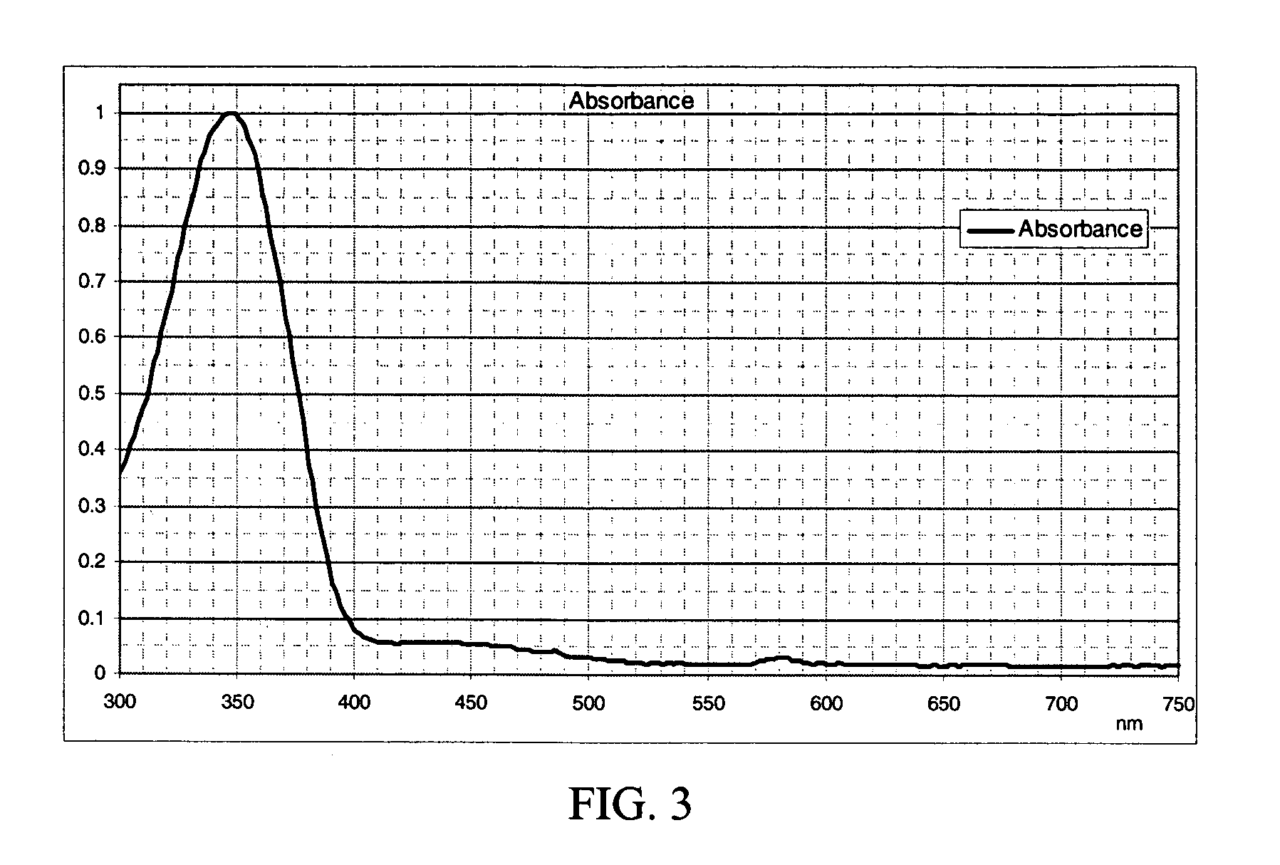
[0022] A new process for forming a laser pixel array for use with a pump-beam involves forming a layer containing a formamide of an amino dye compound on a support, wherein the layer absorbs light outside the laser wavelength and predominantly outside the pump-beam wavelength range. The layer is then subjected to UV radiation in the areas of the layer where it is desired to be free of pixels for a time sufficient to shift the absorption envelope of the layer into the pump-beam wavelength range.

[0023] In one embodiment the pump-beam is part of an Organic VCSEL device. FIG. 1 schematically represents an illustrative example of such a device. The substrate 110 can either be light transmissive or opaque, depending on the intended directions of optical pumping or laser emission. The substrate 110 may be transparent glass or plastic. Alternatively, opaque substrates including, but not limited to, semiconductor materials (e.g., silicon) or ceramic materials may be used in the case where o...


PUM

PropertyMeasurementUnit
pump-beam aaaaaaaaaa
laser wavelengthaaaaaaaaaa
wavelengthaaaaaaaaaa

Abstract

The invention includes a process for forming a laser pixel array useful with a pump-beam, comprising: a) forming a layer containing a formamide of an amino dye compound on a support wherein the layer absorbs light outside the laser wavelength and predominantly outside the pump-beam wavelength range; and b) subjecting the layer to UV radiation in the areas of the layer where it is desired to be free of pixels for a time sufficient to shift the absorption envelope of the areas into the pump-beam wavelength range. The invention also provides for unimolecularly forming an image or an information record and a composition of matter. The invention provides methods for forming filters, images or information records having a smooth surface and in particular for forming a pixel region pattern for use with an Organic VCSEL that would ease manufacturing.

Description

FIELD OF THE INVENTION [0001] This invention relates to a layer and a unimolecular reaction process for selective formation of a pattern of shifted light absorption useful to make a laser pixel array for use with a pump-beam, as a filter array having a smooth surface, and as an information record. A formamide of an amino dye compound is useful to form such a layer. BACKGROUND OF THE INVENTION [0002] Vertical cavity surface emitting lasers (VCSELs) based on inorganic semiconductors (e.g., AlGaAs) have been developed since the mid-80's (K. Kinoshita et al., IEEE J. Quant. Electron. QE-23, 882 (1987)). They have reached the point where AlGaAs-based VCSELs emitting at 850 nm are manufactured by a number of companies and have lifetimes beyond 100 years (K. D. Choquette et al., Proc. IEEE 85, 1730 (1997)). With the success of these near-infrared lasers in recent years, attention has turned to other inorganic material systems to produce VCSELs emitting in the visible wavelength range (C. W...

Claims


Application Information

Patent Timeline
Patent Type & Authority Applications(United States)
IPC IPC(8): G11B7/24G03C5/16
CPCC09B55/002H01S5/423H01S5/36H01S5/18383
Inventor VARGAS, J. RAMONKONDAKOV, DENIS Y.KAHEN, KEITH B.
Owner EASTMAN KODAK CO
Why Eureka
Try Eureka