
Hermetic seal cover and manufacturing method thereof

a technology of sealing cover and manufacturing method, which is applied in the direction of manufacturing tools, basic electric elements, and welding apparatus, to achieve the effect of reducing the incidence of defective joints of seal covers, eliminating such damage to semiconductor devices, and curbing the deterioration of production yield

Active Publication Date: 2006-01-05
TANAKA PRECIOUS METAL IND
View PDF10 Cites 4 Cited by
  • Summary
  • Abstract
  • Description
  • Claims
  • Application Information

AI Technical Summary

Benefits of technology

[0013] In the present invention, the Ni—Sn alloy layer provided preliminarily as a barrier layer between the Ni plating layer and the Au—Sn brazing material layer inhibits alloying of the Ni plating layer and a molten brazing material. The Ni—Sn alloy layer is an intermetallic compound, which protects the Ni plating layer without melting even when the Au—Sn brazing material melts, and inhibits a reaction between Ni plating layer and the brazing material. Thus, according to the present invention, no outgas will be generated when a brazing material is molten during a process of joining a seal cover, and no voids will remain at a joint after joining or solidification.
[0014] Thickness of the Ni—Sn alloy layer as a barrier layer preferably ranges between 0.6 μm and 5.0 μm. Any Ni—Sn alloy layers having a thickness smaller than 0.6 μm will be hard to function as a barrier layer. This is because nickel and brazing material show an alloying reaction albeit only slightly, thereby generating outgas. In contrast, any alloy layers having a thickness exceeding 5.0 μm will be hard to be formed uniformly, thereby fluctuating easily in height of a cover.
[0015] It is preferable if the Au—Sn brazing material of the seal cover according to the present invention shows a substantially eutectic structure. The reason a brazing material having a eutectic structure is preferable is that a melting point is stable in joining, and melting and solidifying of the brazing material can be effected quickly, whereby efficient manufacturing of packages can be achieved. Furthermore, such a brazing material has good wettability, and can form joints with fewer defects. The present inventors propose 20.65-23.5 wt % of Sn—Au as a preferable composition for a Au—Sn brazing layer.
[0019] Formation of the Ni alloy layer on the seal cover main body is made according to a method, which is not different from the conventional ones in particular. The thickness of the Ni plating layer is generally adjusted to 0.5-3 μm, and the present invention also follows suit. Some plating methods including an electrolytic barrel plating are applied as a method of Ni plating. Au plating may be applied onto the surface of the Ni plating layer subsequent to Ni plating. The Au plating is carried out in order to further improve the wettability of the brazing material during fusing the Au—Sn brazing material. It should be noted the Au plating is integrated with the brazing material during fusion of the brazing material, whereby affecting nothing to a formation a Ni—Su alloy layer. Au plating layer is preferably applied with a thickness of 0.01-1.0 μm.
[0023] The above-described hermetic seal cover of the present invention does not generate any outgas during a joining step in manufacture of a packages, whereby the incidence of defective joint of a seal cover will be substantially decreased. In this connection, the conventional hermetic seal covers has been involving risk of damaging semiconductor devices in a package due to outgas, especially a problem of decreasing vibration frequency of a quartz oscillator due to outgas adsorbed thereon. The present invention eliminates such damage to semiconductor devices. Thus, the present invention can curb deterioration of production yield as well as rise in a product cost in mass production of semiconductor packages, which are expected to expand in demand to the future.

Problems solved by technology

However, the number of semiconductor packages mass produced with the popularization of various electronic equipment is quite a few even if the proportion is small, and a loss suffered thereby should not be left disregarded.

Method used


Image

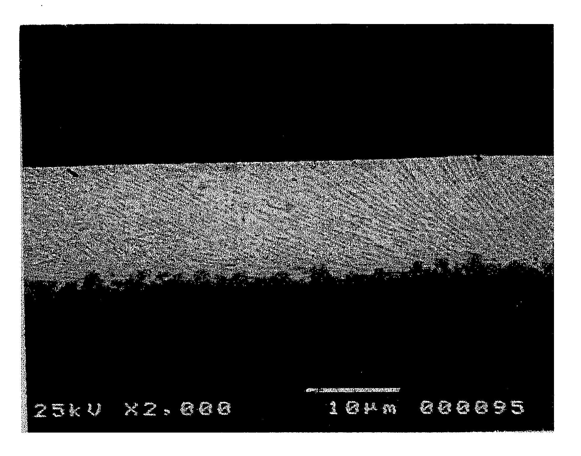
  • Hermetic seal cover and manufacturing method thereof
  • Hermetic seal cover and manufacturing method thereof
  • Hermetic seal cover and manufacturing method thereof

Examples


Embodiment Construction

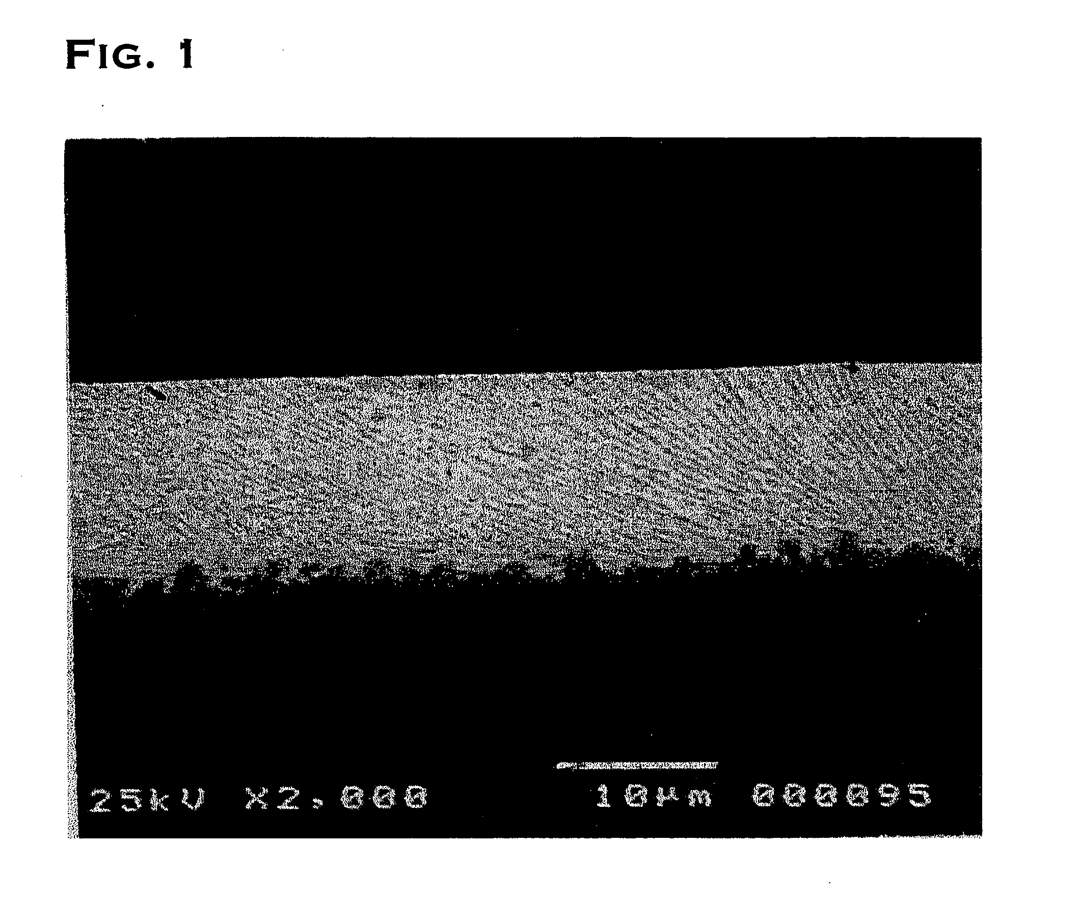
[0027] Hereinafter, preferred embodiments of the present invention will be concretely described. In the embodiments, Au—Sn brazing materials of various compositions were used to manufacture hermetic seal covers with the conditions of fusion bonding changed, each structure was observed, and further packages were manufactured for studying failure rate.

[0028] The seal covers were manufactured in a manner as follows. On a seal cover main body (Size: 3.5 mm×3.5 mm0.1 ×mm) made of KOVAR, 2.0 μm of Ni and 0.1 μm of Au were plated through electrolytic barrel plating. Then, a frame of Au—Sn brazing material (Size: 5 mm Sq.×2.5 mm Sq., 0.05 mm in thickness) was fusion bonded to the seal cover main body under various conditions to manufacture a seal cover. Fusion bonding of the brazing material was effected by positioning and placing the brazing material on the seal cover main body, subsequently inserting the same into an electric furnace for heating for a predetermined period of time.

[0029]...


PUM

PropertyMeasurementUnit
temperatureaaaaaaaaaa
thicknessaaaaaaaaaa
thicknessaaaaaaaaaa

Abstract

A hermetic seal cover capable of inhibiting defects such as voids from generating in sealing a package, and a method of manufacturing the seal cover are provided. The hermetic seal cover comprises: a seal cover main body; a Ni plating layer applied onto a surface of the seal cover main body; and a Au—Sn brazing material layer fusion bonded to a surface of the Ni plating layer, and is characterized by a Ni—Sn ally layer disposed between the Ni plating layer and the Au—Sn brazing material layer. It is preferable if the Ni—Sn alloy layer has a thickness of 0.6-5.0 μm. It is also preferable if Au—Sn brazing material layer has a Sn content of 20.65-23.5 wt %.

Description

BACKGROUND OF THE INVENTION [0001] 1. Field of the Invention [0002] The present invention relates to a hermetic seal cover to be used in hermetically sealing a package for various electronic parts. [0003] 2. Description of the Related Art [0004] Semiconductor devices such as SAW filters and quartz oscillators, which are used in various electronic appliances for, for instance a cellular phone are normally used with the devices enclosed in a ceramic-made container (package), which prevents oxidation or deterioration due to moisture or oxygen. The semiconductor package comprises: a container (base), which has openings and hermetically seals devices; and a seal cover acting as a lid. A process for hermetically sealing a semiconductor package is effected through placing semiconductor devices on a base, placing a seal cover on the devices, and subsequently joining the base and the seal cover. [0005] A typical method out of various ones for joining a base and a seal cover is a brazing meth...

Claims


Application Information

Patent Timeline
Patent Type & Authority Applications(United States)
IPC IPC(8): H01L23/48H01L21/20H01L23/04H01L23/10
CPCH01L23/10H01L2924/01079H01L2924/0002H01L2924/00
Inventor MIYAZAKI, KENICHIKUSAMORI, HIROYUKI
Owner TANAKA PRECIOUS METAL IND
Learn More