
Microscope

a microscope and microscope technology, applied in the field of microscopes, can solve the problems of destroying the detector, generating high-intensity radiation in the specimen being examined, and too much radiation striking the detector to be processed by the detector, so as to avoid the negative impact of the detector

Inactive Publication Date: 2005-12-29
LEICA MICROSYSTEMS CMS GMBH
View PDF7 Cites 3 Cited by
  • Summary
  • Abstract
  • Description
  • Claims
  • Application Information

AI Technical Summary

Benefits of technology

[0006] It is an object of the present invention to provide a microscope of the aforesaid kind with which interference-free image acquisition is possible and negative impact on the detector is avoided, even in the presence of critical investigative parameters such as a high scanning speed and / or strong excitation radiation during bleaching operations.
[0008] What has been recognized according to the present invention is firstly that in certain microscopic investigative methods, the quantity of detected radiation proceeding from the specimen and striking the detector represents a critical variable in terms of both the quality of the acquired image and damage to the detector. To prevent such damage, according to the present invention there is provided in the detection beam path an activatable element with which the detected radiation striking the detector can be regulated and / or limited. The arrangement according to the present invention eliminates, for example, the need to reduce the light intensity in the illumination beam path. An interference-free image can be acquired with reduced light intensity even when the fluorescence is very strong and scanning is very fast (including, for example, during a bleaching operation).
[0009] In a preferred embodiment, a rapidly switchable element is provided, “rapidly” in this context meaning that a time synchronization is possible between the scanning operation on the one hand and switching operations in the controllable element on the other hand. If the switchability is sufficiently rapid, the element can be switched during a scanning operation not only frame-by-frame or line-by-line, but on a pixel-by-pixel or even sub-pixel basis. Pixel- or sub-pixel-based switchability of the controllable element means that the quantity of radiation striking the detector can be regulated with extremely high accuracy, so that overmodulation of the detector can be effectively avoided during the entire scanning operation.
[0014] A liquid crystal display (LCD) or a liquid crystal tunable filter (LCTF) can also be used instead of an acoustooptical element to regulate the light power level of the fluorescent light present in the detection beam path.
[0016] For simple applications, particularly those in which wavelength-specific attenuation is not necessary, a galvanometer can be used as the controllable element.
[0017] In the interest of good flexibility for the arrangement, several, preferably two, controllable elements can be provided as an alternative to the use of a single controllable element in the detection beam path. For example, a first controllable element could be selected so that it specifically allows scattered excitation light to be blocked out, while the second controllable element could be designed for wavelength-specific suppression of fluorescent light.

Problems solved by technology

In some applications, in particular in some fluorescence experiments, the problem occurs that high-intensity radiation is generated in the specimen being examined, and high-intensity detected light is thus guided along the detection beam path to the detector.
It may happen in this context that the quantity of radiation striking the detector is too great to be processed by the detector in the context of its technical capabilities.
In addition to a considerable loss of image quality resulting from nonlinear behavior of the detector caused by the high light intensity, excessive radiation input can also cause damage to the detector or even, in some circumstances, result in complete destruction of the detector.
Specifically, two serious problems may arise in this context: on the one hand, the charge quantities occurring in the photomultiplier may not be dissipated and processed quickly enough because of the high scanning speed in fly mode, resulting in unusable images.
On the other hand, the high intensity of the fluorescent radiation striking the detector can cause damage to the detector, in particular damage to the sensitive photocathode of the photomultiplier.
Excessive stress on the detector can occur in this type of experiment as well, particularly during the bleaching operation.

Method used


Image

  • Microscope
  • Microscope

Examples


Embodiment Construction

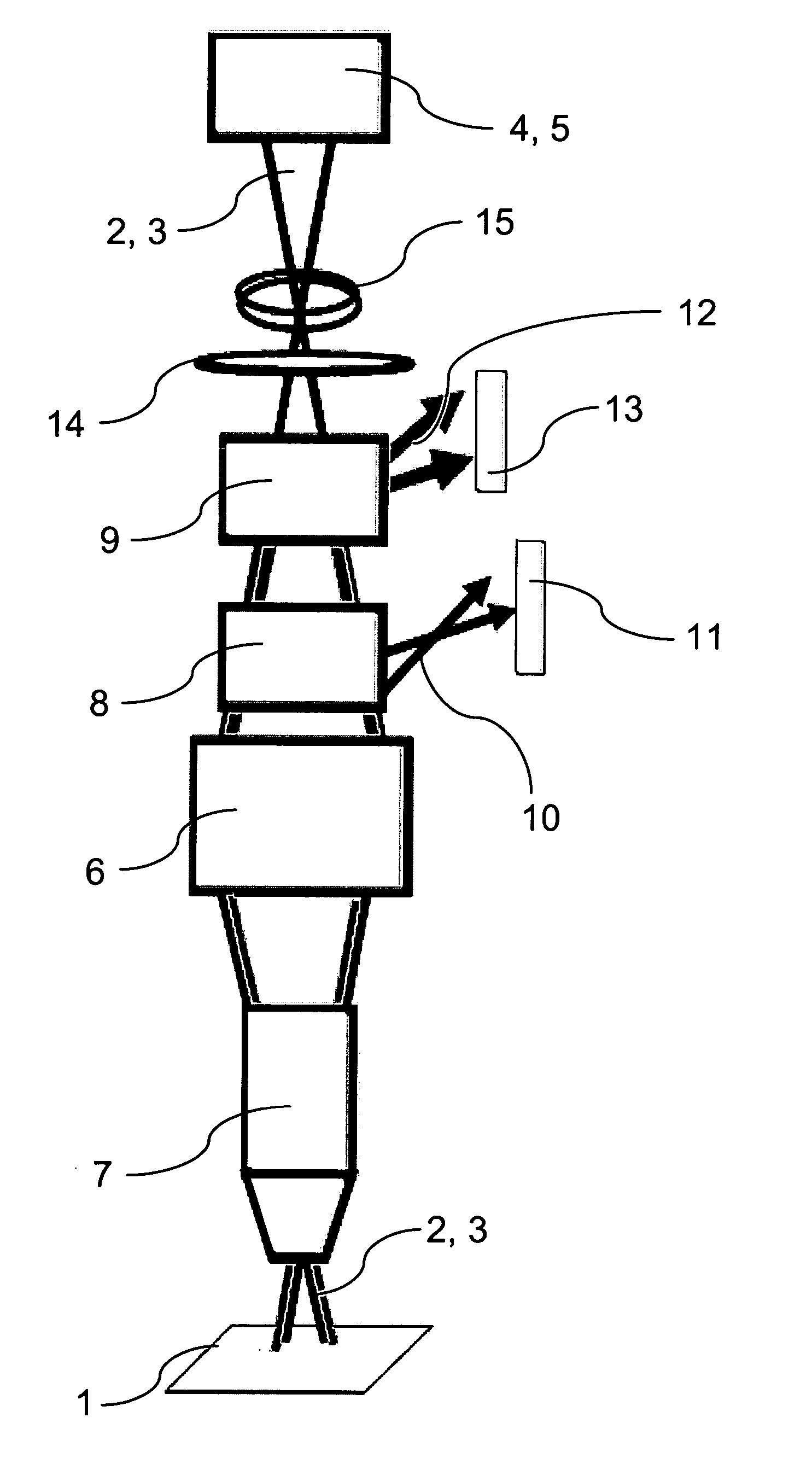
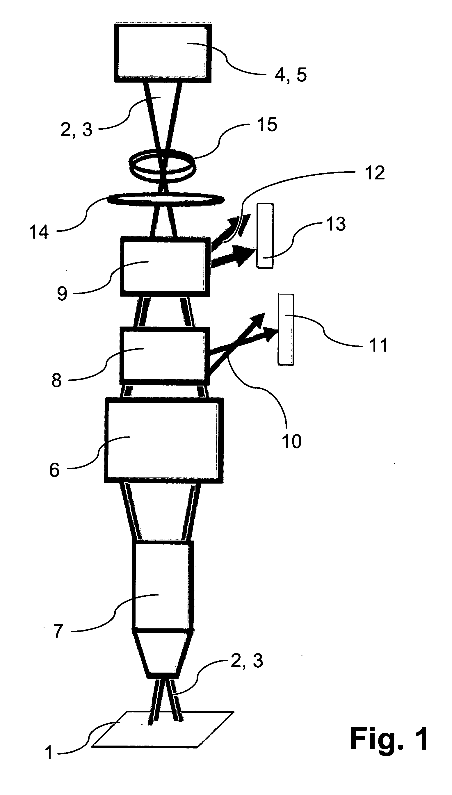
[0023] The Figure schematically shows the general construction of an exemplifying embodiment of a microscope according to the present invention. Detected light 2 proceeding from specimen 1 is guided along a detection beam path 3 to a detector 5 embodied as a photomultiplier 4. The illuminating light is guided along an illumination beam path, via a beam splitter 6 and an objective 7, onto specimen 1. Detected light 2 travels through objective 7 and beam splitter 6 in the reverse order.

[0024] Two controllable elements for regulating and / or limiting the light power level in detection beam path 3 are arranged in front of photomultiplier 4 in detection beam path 3. In the exemplifying embodiment illustrated, these are an AOTF 8 and an AOM 9.

[0025] AOTF 8 is traversed by an acoustic wave that is generated by a piezoacoustic generator activated by a high-frequency source. By modifying the frequency of the waves traveling through AOTF 8, AOTF 8 can be switched in such a way that certain w...


PUM


Abstract

A microscope includes at least one illuminating light source and an illumination beam path for guiding the illuminating light to a specimen. A detection beam path guides detected light from the specimen to a detector. An activatable element is positioned in the detection beam path for regulating and / or limiting the light power level in the detection beam path.

Description

[0001] Priority is claimed to German patent application DE 10 2004 031 048.3, filed Jun. 25, 2004, the entire disclosure of which is hereby incorporated by reference herein. [0002] The invention concerns a microscope, in particular a fluorescence microscope, having at least one light source, an illumination beam path guiding the light to a specimen, a detector, and a detection beam path guiding the detected light from the specimen to the detector. BACKGROUND [0003] Microscopes of the kind under discussion here have been used for a long time in a wide variety of embodiments for numerous different applications. In some applications, in particular in some fluorescence experiments, the problem occurs that high-intensity radiation is generated in the specimen being examined, and high-intensity detected light is thus guided along the detection beam path to the detector. It may happen in this context that the quantity of radiation striking the detector is too great to be processed by the d...

Claims


Application Information

Patent Timeline
Patent Type & Authority Applications(United States)
IPC IPC(8): G02B21/06G02B21/16
CPCG02B21/16
Inventor SEYFRIED, VOLKERKNEBEL, WERNERSCHROEDER, JAN
Owner LEICA MICROSYSTEMS CMS GMBH
Learn More