Temperature compensated bias network

a bias network and temperature compensation technology, applied in the field of electrical circuits, can solve the problems of a very limited electrical operating range of integrated designs for processing analog signals, and achieve the effects of superior performance, high operating frequency, and superior performance results

Active Publication Date: 2005-12-29
SKYWORKS SOLUTIONS INC
View PDF3 Cites 7 Cited by
  • Summary
  • Abstract
  • Description
  • Claims
  • Application Information

AI Technical Summary

Benefits of technology

[0005] Accordingly, the invention provides bias circuits with superior performance including stability in the face of temperature variation. Such bias circuits may be implemented as an IC (integrated circuit) with bipolar transistors as disclosed herein. However the invention is not limited to bipolar devices, nor even necessarily to dense integrated, although that is usual and usually desirable. CMOS or other semiconductor technologies such as SiGe (silicon-germanium), GaAs (Gallium Arsenide) or InP (Indium Phosphate) or other III-IV semiconductor bipolar, HBT (heterojunction bipolar transistor) or FET (field-effect transistor) devices may also be used. High operating frequency (e.g., microwave) may be supported through LSI (large scale integration), as is well-known in the art. Superior performance results from aspects of the novel designs.

Problems solved by technology

Dense and highly integrated designs for processing analog signals often have a very limited electrical operating range and, especially when low voltage power supplies must be conformed to, such circuits may require bias currents (and / or voltages) to be controlled with great precision and robustness.

Method used


Image

  • Temperature compensated bias network
  • Temperature compensated bias network
  • Temperature compensated bias network

Examples


Embodiment Construction

[0024] In the following description, for purposes of clarity and conciseness of the description, not all of the numerous components shown in the schematics and / or drawings are described. The numerous components are shown in the drawings to provide a person of ordinary skill in the art a thorough, enabling disclosure of the present invention. The operation of many of the components would be understood and apparent to one skilled in the art.

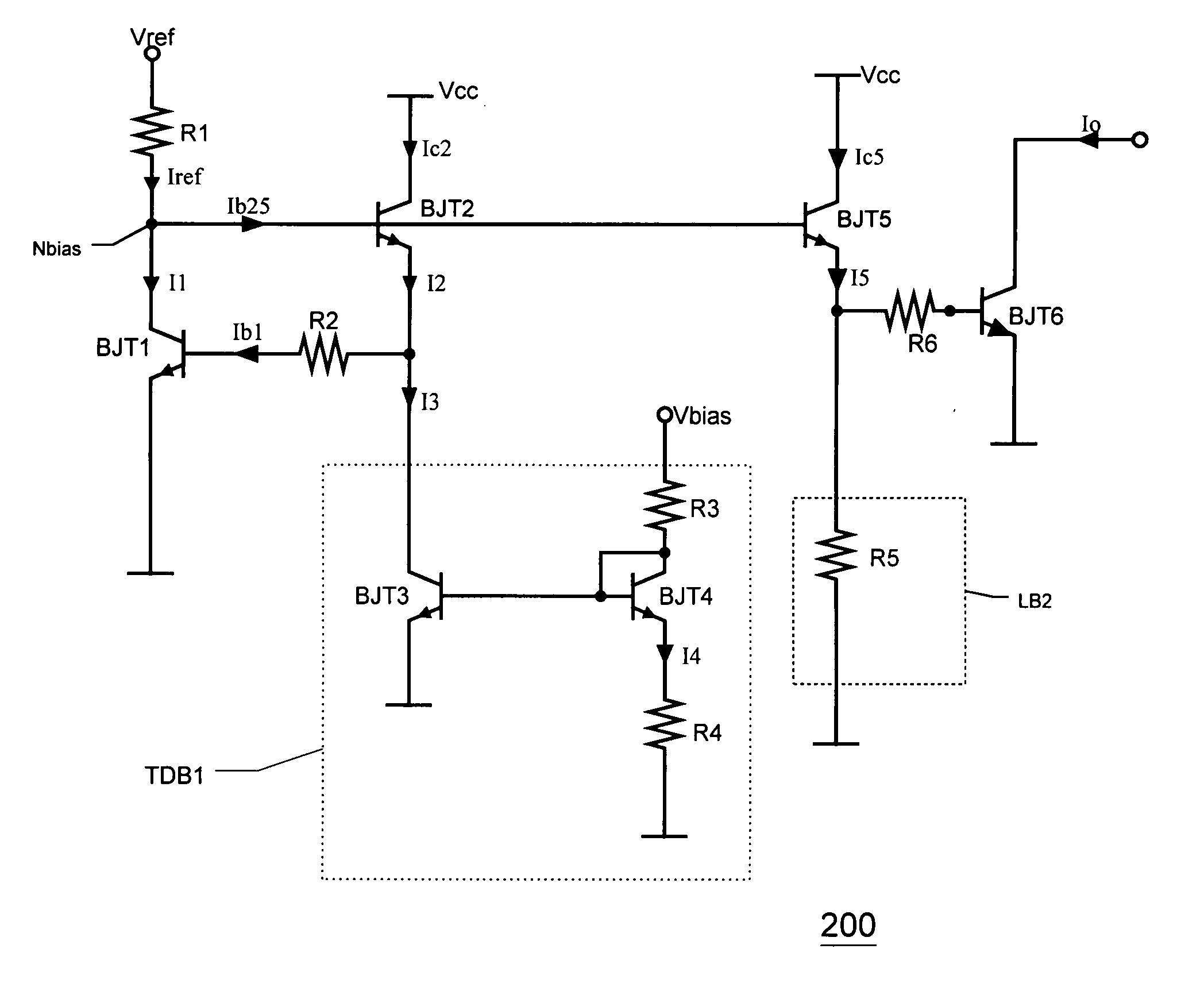
[0025]FIG. 1 is a schematic diagram of a part of an integrated circuit 200 (IC) according to an embodiment of a bias circuit according to an exemplary embodiment of the invention. As shown, IC 200 implements an exemplary analog bias circuit, and in the present example bipolar technologies are used.

[0026] Referring to FIG. 1, the bias network circuit 200 provides a 0 Hz output current Io. In a typical embodiment BJT6 may be a device intended to be biased into an active region so as to act as a transistor that receives an RF input signal, or to cre...


PUM


Abstract

A method and apparatus for a temperature compensated bias network, such as may be embodied as an integrated circuit is disclosed. Embodiments provide for a wide range of desired temperature characteristics with good stability. Current mirror components with active leakage circuits may act to provide consistent operating parameters over a wide range of temperatures. Improved compensation and linearity may be provided using features disclosed.

Description

FIELD OF THE INVENTION [0001] The invention generally relates to electronics circuits. The invention more particularly relates to amplifier circuits, for example, RF (radio frequency) PA (power amplifier) circuits especially integrated circuits for microwave signals. BACKGROUND OF THE INVENTION [0002] Modern designs for high power and high performance ICs (integrated circuits) RF (radio frequency) signals meet their considerable challenges by deploying any of a variety of technologies, often including out of the mainstream techniques. Dense and highly integrated designs for processing analog signals often have a very limited electrical operating range and, especially when low voltage power supplies must be conformed to, such circuits may require bias currents (and / or voltages) to be controlled with great precision and robustness. [0003] Superior control of bias voltages across a wide range of operating conditions such as temperature may be achieved by exploiting refinements disclose...

Claims


Application Information

Patent Timeline
Patent Type & Authority Applications(United States)
IPC IPC(8): G05F3/16G05F3/22H03F3/45
CPCG05F3/225
Inventor RATEGH, HAMID REZAHOZOURI, BEHZAD TAVASSOLI
Owner SKYWORKS SOLUTIONS INC
Why Eureka
Try Eureka