In-plane switching mode liquid crystal display device
a liquid crystal display and switching mode technology, applied in non-linear optics, instruments, optics, etc., can solve problems such as lowering picture quality, and achieve the effect of preventing the distortion of transverse electric fields
- Summary
- Abstract
- Description
- Claims
- Application Information
AI Technical Summary
Benefits of technology
Problems solved by technology
Method used
Image
Examples
first embodiment
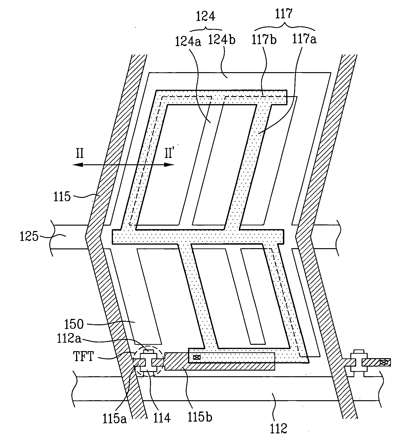
[0037]FIG. 3 is a plane view of an IPS mode LCD device according to an exemplary first embodiment of the present invention. FIG. 4 is a cross sectional view along II-II′ of FIG. 3. FIG. 5 is a plane view of a common electrode in an IPS mode LCD device according to the exemplary first embodiment of the present invention.
[0038] In an IPS mode LCD device according to the first embodiment of the present invention, the number of blocks, each of which is defined with a pixel electrode and a common electrode, may be an odd or even number in direction of a gate line, to improve the degree of freedom on design. Also, the IPS mode LCD device according to the first embodiment of the present invention improves an aperture ratio by optimizing a pixel region. In the IPS mode LCD device according to the first embodiment of the present invention, a line width above 1 μm, preferably, about 3 μm, is decreased in the common electrode overlapped with the pixel electrode, thereby preventing the distort...
second embodiment
[0055]FIG. 11 is a plane view of an IPS mode LCD device according to an exemplary second embodiment of the present invention. FIG. 12 is a plane view of a common electrode in an IPS mode LCD device according to the exemplary second embodiment of the present invention.
[0056] In an IPS mode LCD device according to the second embodiment of the present invention, the number of blocks, which is defined as a pixel electrode and a common electrode, may be an odd or even number in direction of a gate line. In the IPS mode LCD device according to the second embodiment of the present invention, a line width is decreased in the common electrode overlapped with the pixel electrode by more than about 1 μm, preferably by about 3 μm, thereby preventing the distortion of electric field generated in the circumference of outermost common electrode.
[0057] Especially, in the case of the IPS mode LCD device according to the second embodiment of the present invention, as shown in FIG. 11, a data line 2...
third embodiment
[0066]FIG. 13 is a plane view of an IPS mode LCD device according to an exemplary third embodiment of the present invention. FIG. 14 is a plane view of a common electrode in an IPS mode LCD device according to the exemplary third embodiment of the present invention.
[0067] In case of the IPS mode LCD device according to the second embodiment of the present invention, as shown in FIG. 11, the equipotential may be formed in the corners of the common electrode 224 and the pixel electrode 217, and the electric field may be weak due to the long distance between the common electrode 224 and the pixel electrode 217, whereby the transmissivity may be lowered due to the failure of driving the liquid crystal directors.
[0068] To overcome these problems of the IPS mode LCD device according to the second embodiment of the present invention, one part of a pixel electrode 517 is formed in a bent structure in an IPS mode LCD device according to the third embodiment of the present invention. In the...
PUM
 Abstract
Description
Claims
Application Information
 - R&D
- Intellectual Property
- Life Sciences
- Materials
- Tech Scout
- Unparalleled Data Quality
- Higher Quality Content
- 60% Fewer Hallucinations
Browse by: Latest US Patents, China's latest patents, Technical Efficacy Thesaurus, Application Domain, Technology Topic, Popular Technical Reports.
© 2025 PatSnap. All rights reserved.Legal|Privacy policy|Modern Slavery Act Transparency Statement|Sitemap|About US| Contact US: help@patsnap.com


