
Parallel bit testing device and method

a testing device and parallel bit technology, applied in the field of memory devices, can solve the problems of reducing the productivity affecting the use failing to replace the defective memory cells of the memory device,

Inactive Publication Date: 2005-11-17
SAMSUNG ELECTRONICS CO LTD
View PDF9 Cites 11 Cited by
  • Summary
  • Abstract
  • Description
  • Claims
  • Application Information

AI Technical Summary

Problems solved by technology

When both memory cells in a memory cell pair are defective, however, the comparison result may indicate that the memory cells are not defective, and thus the memory device fails to replace the defective memory cells.
Accordingly, the memory device and parallel bit test disclosed above requires the sequential storing of inverted and non-inverted test pattern data into the test pattern data register, which complicates and slows testing, and lowers productivity of the memory device.

Method used


Image

  • Parallel bit testing device and method
  • Parallel bit testing device and method
  • Parallel bit testing device and method

Examples


Embodiment Construction

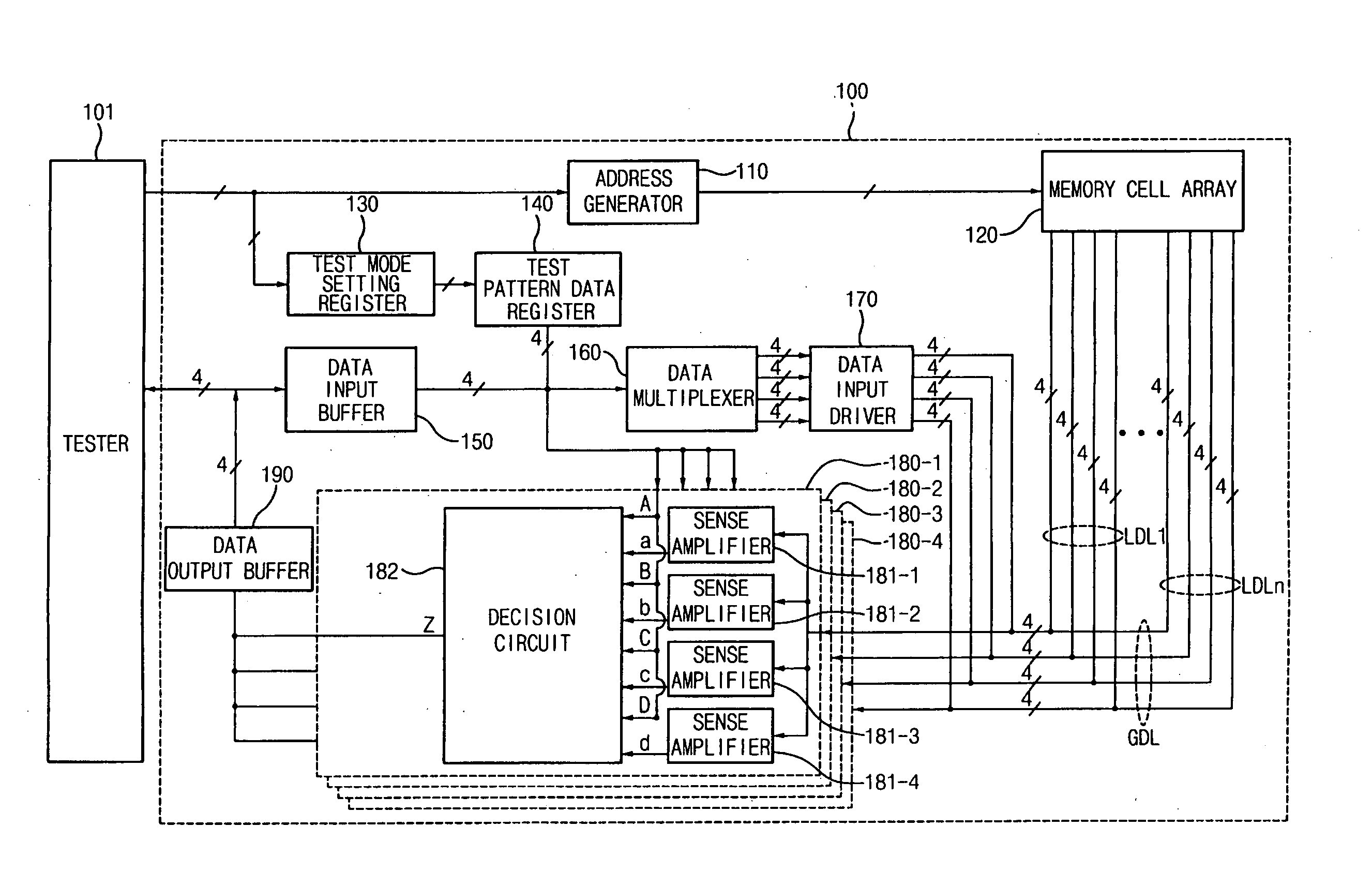
[0018]FIG. 1 is a block diagram showing a memory device according to an embodiment of the present invention. Referring to FIG. 1, a system for performing parallel bit test operations includes a tester 101 and a memory device 100. The memory device 100 includes an address generator 110, a memory cell array 120, a test mode setting register 130, a test pattern data register 140, a data input buffer 150, a data multiplexer 160, a data input driver 170, data output circuits 180-1, 180-2, 180-3 and 180-4, and a data output buffer 190.

[0019] The tester 101 tests the memory cell array 120 by providing an address and test pattern data to the memory device 100. The tester 101 provides the address to the memory cell array 120 via the address generator 110, and provides the test pattern data to the test pattern data register 140 via the data input buffer 150. Alternatively, the test pattern data register 140 may receive the test pattern data from the test mode setting register 130.

[0020] The...


PUM

PropertyMeasurementUnit
time delayaaaaaaaaaa

Abstract

A memory device includes a memory cell array to store data, a register to store test data, and a decision circuit to invert the test data and to determine a failure of at least one memory cell within the memory cell array responsive to the data, the test data, and the inverted test data.

Description

REFERENCE TO RELATED APPLICATIONS [0001] This application claims priority to Korean Patent Application No. 2004-33166, filed on May 11, 2004, which we incorporate by reference. BACKGROUND OF THE INVENTION [0002] 1. Field of the Invention [0003] The present invention relates to memory devices, more particularly, to a parallel bit testing device and method for detecting defective memory cells within memory devices. [0004] 2. Description of the Related Art [0005] A typical memory device includes a memory cell array, where each memory cell in the array may store data. To determine which memory cells, if any, are defective, a tester may perform a parallel bit test on the memory cell array. To perform the parallel bit test, the memory device is configured into a parallel bit test mode responsive to a test mode setting command from the tester. The tester writes test pattern data to the memory cell array, where each memory cell is paired with another memory cell and written with the same da...

Claims


Application Information

Patent Timeline
Patent Type & Authority Applications(United States)
IPC IPC(8): G01R31/28G11C29/00G11C29/10G11C29/34G11C29/40
CPCG11C29/34G11C2029/2602G11C2029/0405G11C29/40A47L17/08
Inventor KIM, HONG-BEOM
Owner SAMSUNG ELECTRONICS CO LTD
Learn More