Adaptive hysteresis receiver for a high speed digital signal

Inactive Publication Date: 2005-10-27
HEWLETT PACKARD DEV CO LP
View PDF5 Cites 6 Cited by
  • Summary
  • Abstract
  • Description
  • Claims
  • Application Information

AI Technical Summary

Benefits of technology

[0012] In another embodiment, a method reduces noise received with a high speed digital signal. The high speed digital signal is compared to a reference voltage to generate an output signal. The output signal is latched, according to a clock signal, to produce a control signal. A reference voltage is generated, from a plurality of voltages defining a deep hysteresis level and a shallow hysteresis level, in response to the output signal and the control signal.
[0013] In anot

Problems solved by technology

With increasing processing speed of digital signals in modern circuits, the effect of noise on these signals becomes increasingly problematic.
These noise problems are further exacerbated when a number of digital circuits connect to a single bus and receive the same signal.
In signals where the information content is coincident with the edge of the waveform (e.g., where the edge of a strobe signal is used to latch data and/or clock state machines), a “glitch” can nonetheless cause a significant problem.
Often, therefore, the noise level increases above the hysteresis level; noise then transfers through the hysteresis receiver circuits.
The use of ‘deep’ hysteresis levels, where the amount of input hysteresis is large, also reduces the response time of the hysteresis receiver circuit since the input signal takes longer to reach the transition threshold levels.
Where the deep hysteresis levels are close to the maximum input signal levels, any reduction in input si

Method used


Image

  • Adaptive hysteresis receiver for a high speed digital signal
  • Adaptive hysteresis receiver for a high speed digital signal
  • Adaptive hysteresis receiver for a high speed digital signal

Examples


Example

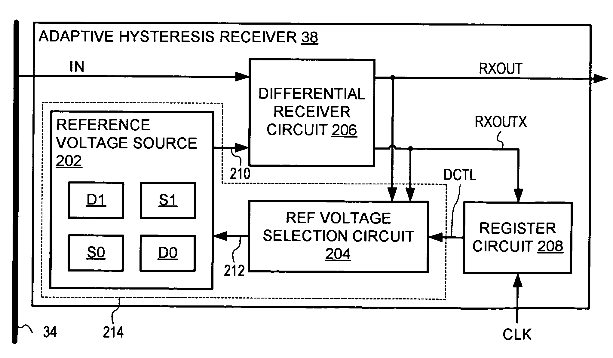
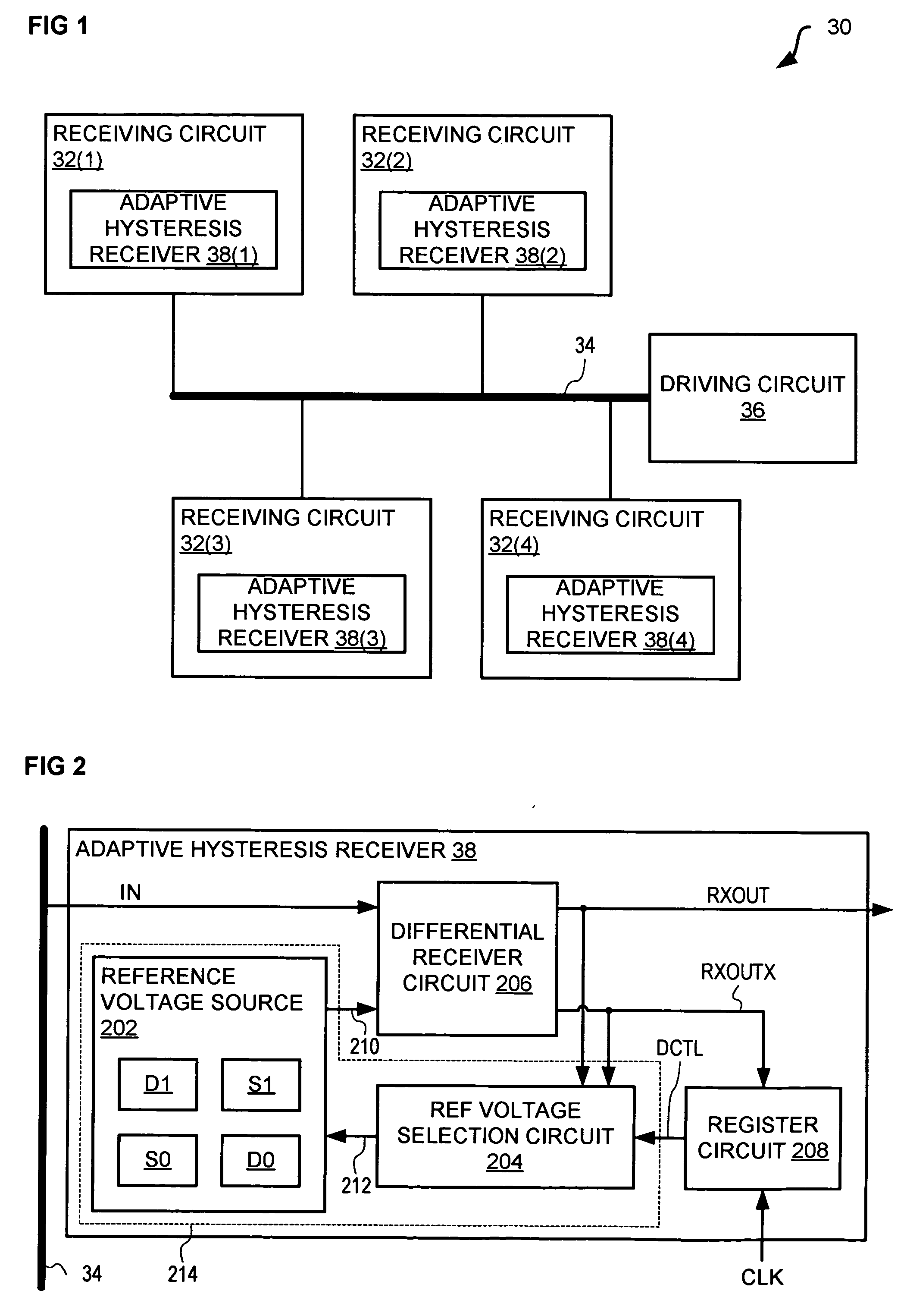
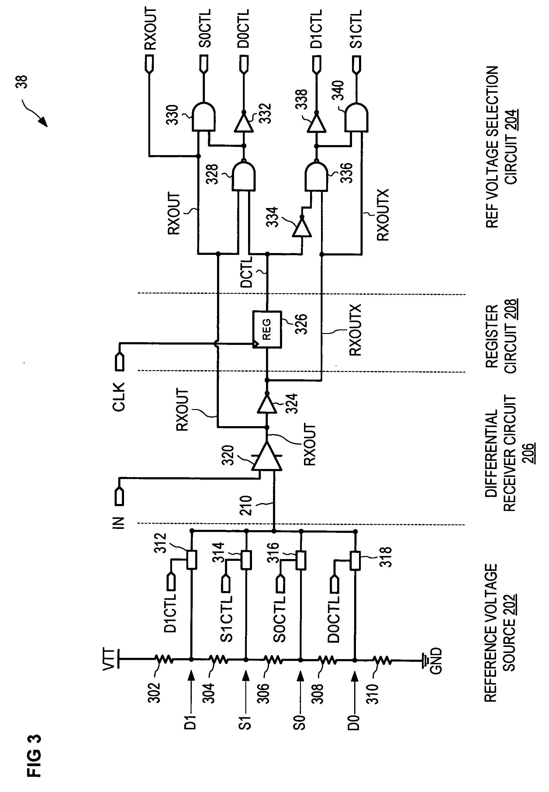
DETAILED DESCRIPTION OF THE FIGURES

[0030]FIG. 1 illustrates an exemplary embodiment of one system 30 that has four receiving circuits 32 connected to a single bus 34 driven by a driving circuit 36. Each receiving circuit 32 has at least one adaptive hysteresis receiver 38, such as shown. More or fewer receiving circuits 32 and adaptive hysteresis receivers 38 may exist depending upon the desired application.

[0031] In operation, driving circuit 36 generates high speed digital signals on bus 34. These high speed digital signals may have varying amounts of noise (e.g., unwanted signals) at different positions on bus 34. Each adaptive hysteresis receiver 38 receives one of the high speed digital signals of bus 34, and operates to ignore noise for that one signal. Accordingly, although not shown, each receiving circuit 32 may have a plurality of adaptive hysteresis receivers 38 so that receiving circuit 32 can receive multiple noise-free signals from bus 34.

[0032] Bus 34 may represent...


PUM


Abstract

An adaptive hysteresis receiver processes a high speed digital signal. A differential receiver circuit compares the high speed digital signal to a reference voltage to generate an output signal. A register circuit latches the output signal, according to a clock signal, to produce a control signal. A reference voltage generator generates the reference voltage, from a plurality of voltages defining a deep hysteresis level and a shallow hysteresis level, in response to the output signal and the control signal.

Description

BACKGROUND [0001] With increasing processing speed of digital signals in modern circuits, the effect of noise on these signals becomes increasingly problematic. These noise problems are further exacerbated when a number of digital circuits connect to a single bus and receive the same signal. [0002] Many techniques have been employed to reduce noise sensitivity of such circuits. In signals where the information content is coincident with the edge of the waveform (e.g., where the edge of a strobe signal is used to latch data and / or clock state machines), a “glitch” can nonetheless cause a significant problem. A glitch is a short pulse or noise spike to which circuit response is not desired. A two-dimensional de-glitch filter may, for example, be used for these types of signal, such as described in U.S. patent application Ser. No. 10 / 653,341, filed on Sep. 2nd, 2003 and incorporated herein by reference. [0003] In signals where information content is determined by signal level and a dat...

Claims


Application Information

Patent Timeline
IPC IPC(8): H03K5/08H03K5/1252H03K9/00H04L25/06H04L25/08
CPCH03K5/082H04L25/063H03K5/1252
Inventor ZHU, ZHUBIAOKOCH, KENNETH IIJOHNSON, DAVID J.C.
Owner HEWLETT PACKARD DEV CO LP
Why Eureka
Try Eureka