
Verification of integrated circuit tests using test simulation and integrated circuit simulation with simulated failure

Active Publication Date: 2005-10-13
ADVANTEST CORP
View PDF10 Cites 16 Cited by
  • Summary
  • Abstract
  • Description
  • Claims
  • Application Information

AI Technical Summary

Benefits of technology

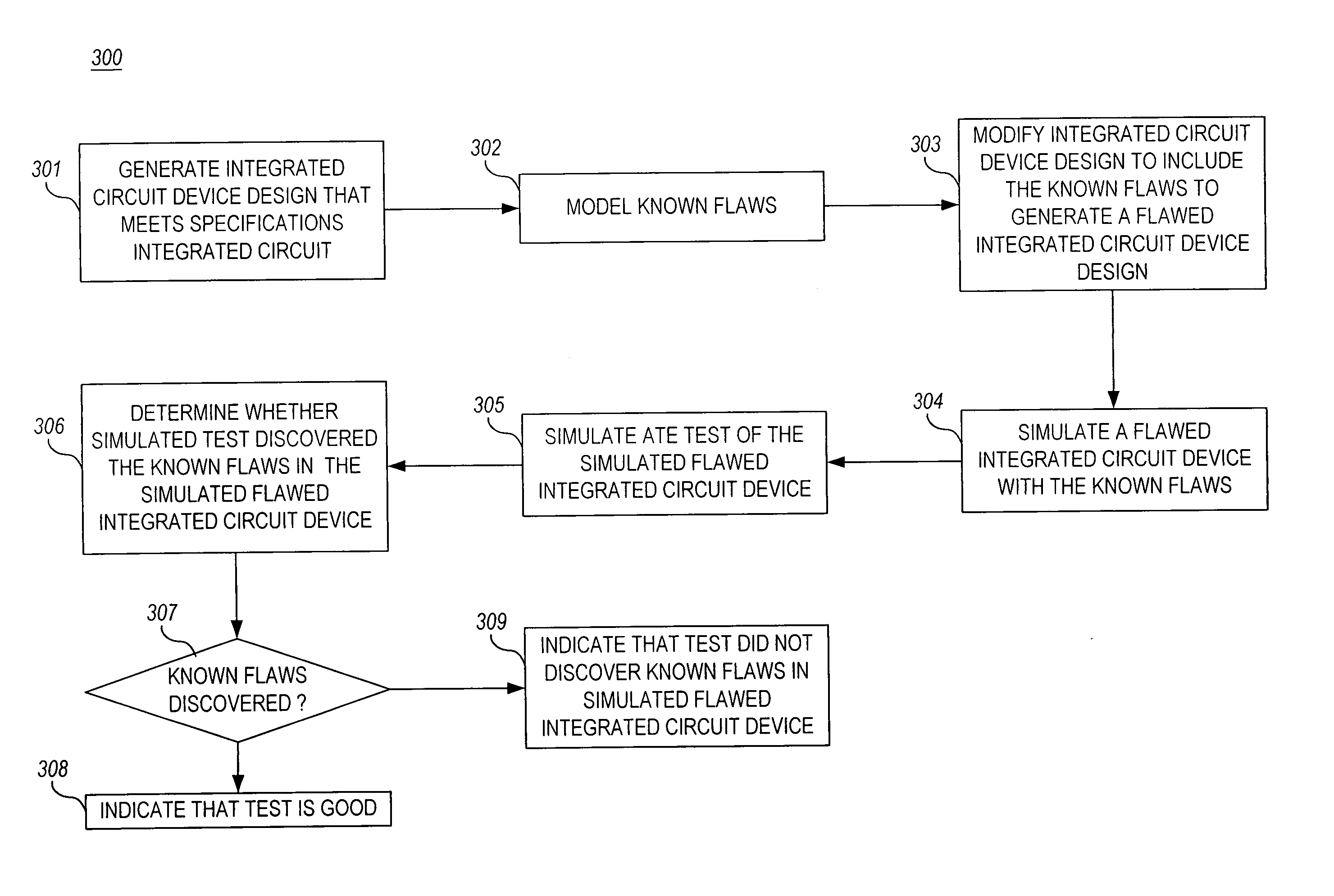
The present invention is a method and apparatus for testing integrated circuit devices to detect flaws with known defects before actually executing the test on an actual integrated circuit device tester. This is done by modifying the integrated circuit device design to model the known defects and simulating the test using a tester simulator and a flawed integrated circuit device simulator. If the simulated test detects the known flaws in the flawed integrated circuit device and fails it, the test is considered good for failing similarly flawed physical embodiments of the integrated circuit device to be tested. This approach allows manufacturing problems to be simulated during virtual test and easily verify that their ATE tests detect common expected problems prior to actual availability of the physical embodiments of the integrated circuit devices.

Problems solved by technology

Typical flaws are due to process variations, dust, chemical contaminants, and other factors.

Method used


Image

  • Verification of integrated circuit tests using test simulation and integrated circuit simulation with simulated failure
  • Verification of integrated circuit tests using test simulation and integrated circuit simulation with simulated failure
  • Verification of integrated circuit tests using test simulation and integrated circuit simulation with simulated failure

Examples


first embodiment

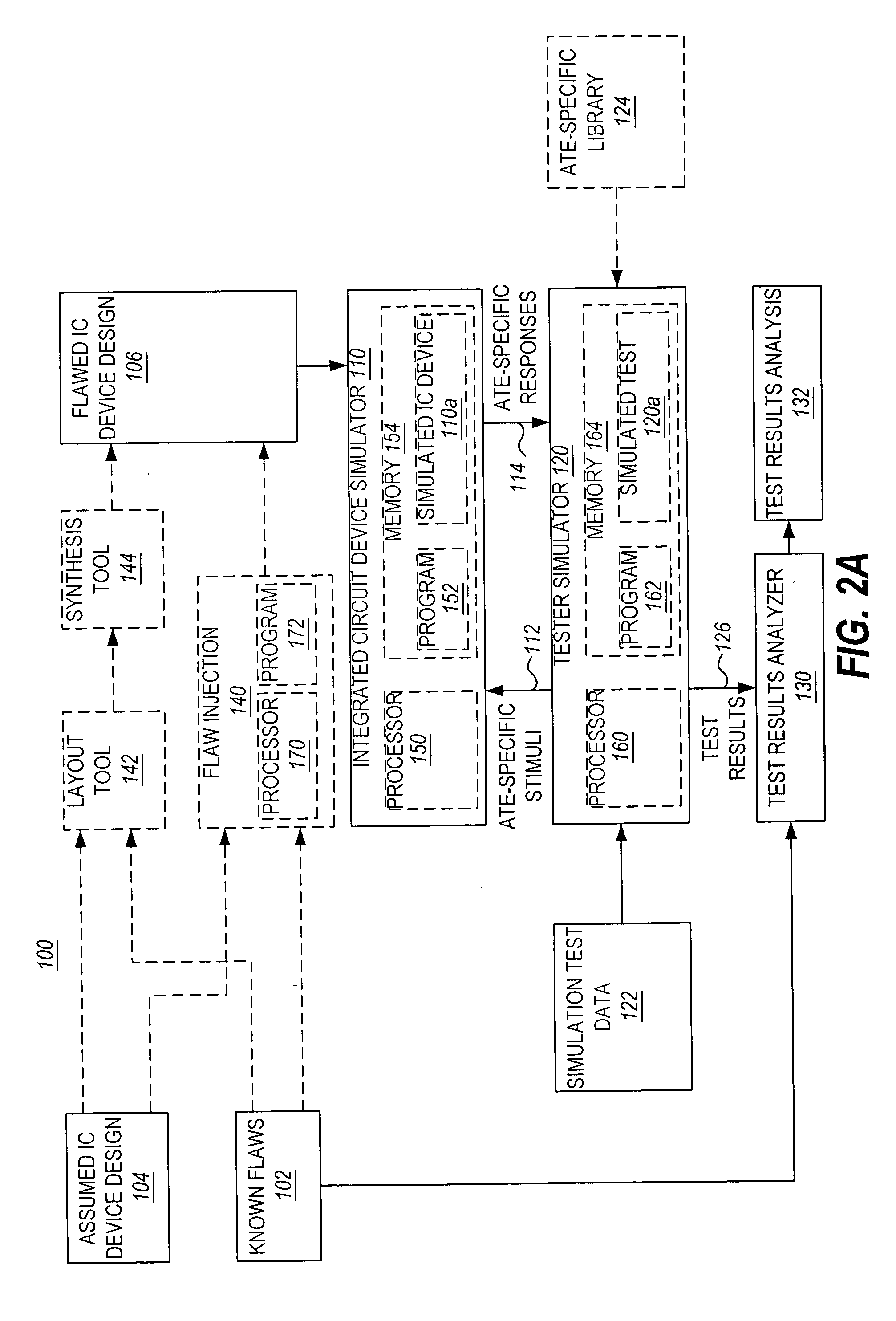
[0029] Turning now to the invention, FIG. 2A is a block diagram of a resimulation tool 100 implemented in accordance with the invention which verifies the ability of an integrated circuit device test to fail bad parts with known defects prior to actual execution of the test on the real integrated circuit device tester. Resimulation tool 100 includes an integrated circuit device simulator 110 and a tester simulator 120.

[0030] The integrated circuit device simulator 110 comprises a processor 150 that executes a simulation program 152 stored in memory 154 that simulates an intentionally flawed integrated circuit device 110a synthesized according to an intentionally flawed integrated circuit device design 106. This can be effected according to one of two preferred methods. In the first method, exemplified in the first embodiment of the resimulation tool 100 of FIG. 2A, the assumed good integrated circuit device design 104 (i.e., the design according to which the physical embodiment of t...

second embodiment

[0040] The second method for simulating an intentionally flawed integrated circuit device synthesized according to an intentionally flawed integrated circuit device design 106 is illustrated in the resimulation tool 200, shown in FIG. 2B. In this embodiment, the assumed good integrated circuit device design 104 and set of known integrated circuit device flaws 102 that model one or more known defects of the integrated circuit device are each input directly to a “smart” integrated circuit device simulator 210. The “smart” integrated circuit device simulator 210 integrates the known flaws into the assumed integrated circuit device design 104 during simulation to simulate a flawed integrated circuit device 210a.

[0041] The operation of the “smart” integrated circuit device simulator 210 as seen by the tester simulator 120 is similar to that of the integrated circuit device simulator 110 of FIG. 110 from the perspective of the tester simulator 120 in that the “smart” integrated circuit d...


PUM


Abstract

A method and apparatus for verifying an integrated circuit device test for testing an integrated circuit device on an automated tester is presented. An integrated circuit device simulator simulates a flawed integrated circuit device that models one or more known flaws, or physical defects, in an assumed good integrated circuit device design. A tester simulator simulates the integrated circuit device test which sends stimuli to, and receives responses from, the simulated flawed integrated circuit device. A test analyzer then determines whether the simulated test of the simulated flawed integrated circuit device detected the flaws in the simulated flawed integrated circuit device and properly failed the simulated flawed integrated circuit device.

Description

BACKGROUND OF THE INVENTION [0001] The present invention relates generally to electronic circuit testing, and more particularly to a method and system for verifying the reliability of an integrated circuit device test using test simulation and integrated circuit device sin with simulated integrated circuit flaws representative of known integrated circuit defects. [0002] The increasing reliance upon computer systems in every industrial and economic sector has led to the continuous improvement of the system hardware and associated processes that run on the hardware. While smaller processes, increased density, and faster speeds of integrated circuits have revolutionized the size and capability of today's computerized products, these same integrated circuit improvements have dramatically increased the cost and complexities of designing and testing such devices. [0003] Currently, integrated multi-functional Electronic Automation Design (EAD) tools are used to design and simulate integrat...

Claims


Application Information

Patent Timeline
Patent Type & Authority Applications(United States)
IPC IPC(8): G01R35/00G01R31/28G01R31/3183G06F17/50H01L21/82
CPCG01R31/318357
Inventor HILDEBRANT, ANDREW S.
Owner ADVANTEST CORP
Learn More