
Micro-switching device and method of manufacturing micro-switching device

Inactive Publication Date: 2005-10-13
FUJITSU LTD
View PDF4 Cites 31 Cited by
  • Summary
  • Abstract
  • Description
  • Claims
  • Application Information

AI Technical Summary

Benefits of technology

[0014] The present invention has been proposed under the circumstances described above. It is therefore an object of the present invention to provide a micro-switching device suitable for reducing the insertion loss. Another object of the present invention is to provide a method of manufacturing such a micro-switching device.
[0017] The stationary contact electrodes in the device of the present invention may be formed, for example, by depositing or growing a material using a plating method on the side opposite to the base substrate via the extending part. The thickness of the stationary contact electrodes can thus be set sufficiently great to realize the desired low resistance. Such a micro-switching device is suitable for reducing the insertion loss.
[0020] Preferably, the extending part may be made of monocrystalline silicon so as to suppress internal stress in the extending part. The internal stress is unfavorable since it can cause deformation of the extending part. Preferably, the extending part may have a thickness of at least 5 μm, i.e. no smaller than 5 μm. This arrangement is suitable for suppressing unwanted deformation of the extending part.

Problems solved by technology

However, with the micro-switching device X4 described above, it is difficult to make the stationary contact electrodes 404 thick, and in actual practice the thickness of the stationary contact electrodes 404 is about 2 μm at most.
With the micro-switching device X4, it may thus be difficult to realize a sufficiently low resistance for the stationary contact electrodes 404, and as a result it may not be possible to realize a low insertion loss.

Method used


Image

  • Micro-switching device and method of manufacturing micro-switching device
  • Micro-switching device and method of manufacturing micro-switching device
  • Micro-switching device and method of manufacturing micro-switching device

Examples


first embodiment

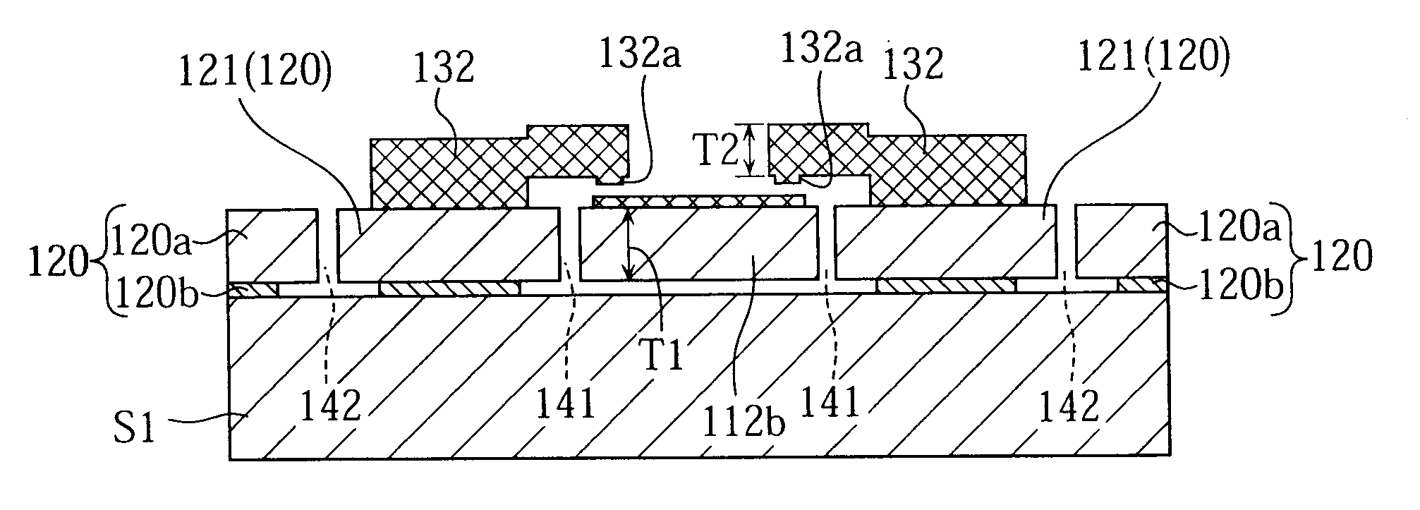
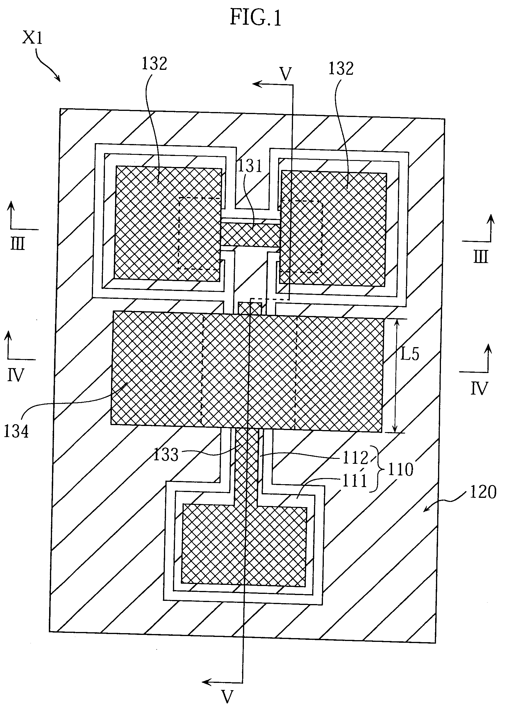
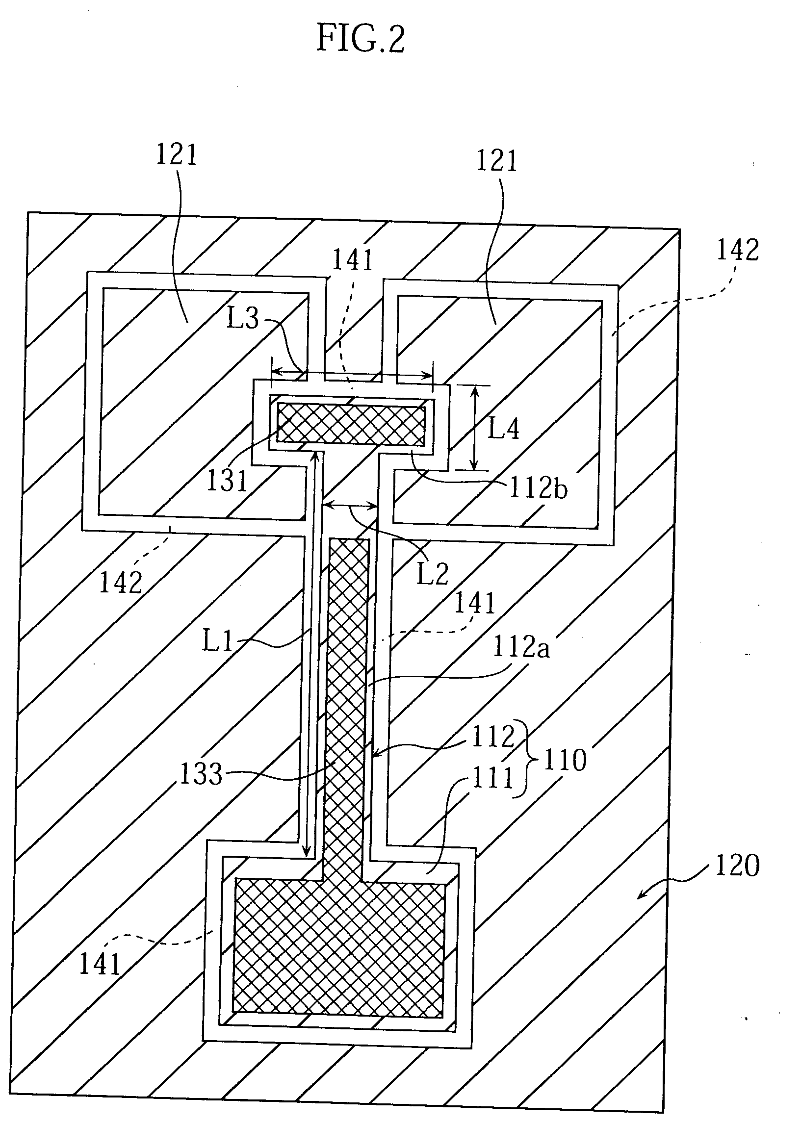
[0061] FIGS. 1 to 5 show a micro-switching device X1 according to the present invention. FIG. 1 is a plan view of the micro-switching device X1, FIG. 2 is a plan view of the micro-switching device X1 with some parts omitted, and FIGS. 3 to 5 are respectively sectional views along lines III-III, IV-IV and V-V in FIG. 1.

[0062] The micro-switching device X1 includes a base substrate S1, a movable cantilever portion 110, a fixing member 120, a movable contact conductor 131, a pair of stationary contact electrodes 132 (omitted from FIG. 2), a first driving electrode 133, and a second driving electrode 134 (omitted from FIG. 2).

[0063] The movable cantilever portion 110 has an anchor part 111 and an extending part 112. As shown in FIG. 5, the anchor part 111 has a layered structure having a main layer 111a and a boundary layer 111b, and is joined to the base substrate S1 on the boundary layer 111b side. As shown for example in FIGS. 2 and 5, the extending part 112 has a body 112a and a he...

second embodiment

[0088] FIGS. 13 to 16 show a micro-switching device X2 according to the present invention. FIG. 13 is a plan view of the micro-switching device X2, FIG. 14 is a plan view of the micro-switching device X2 with some parts omitted, and FIGS. 15 and 16 are respectively sectional views along lines XV-XV and XVI-XVI in FIG. 13.

[0089] The micro-switching device X2 includes a base substrate S2, four movable cantilever portions 210, a fixing member 220, four movable contact conductors 231, a common contact electrode 232 (omitted from FIG. 14), four stationary individual contact electrodes 233 (omitted from FIG. 14), four first driving electrodes 234, and two second driving electrodes 235 (omitted from FIG. 14). The micro-switching device X2 is provided with four micro-switching devices X1 of the first embodiment.

[0090] Each of the movable portions 210 has an anchor part 211 and an extending part 212. As with the anchor part 111 described earlier, the anchor part 211 has a layered structure ...

third embodiment

[0099] FIGS. 17 to 19 show a micro-switching device X3 according to the present invention. FIG. 17 is a plan view of the micro-switching device X3. FIG. 18 is a plan view of the micro-switching device X3 with some parts omitted, and FIG. 19 is a sectional view along line XIX-XIX in FIG. 18.

[0100] The micro-switching device X3 includes a base substrate S3, a movable cantilever portion 110, a fixing member 120, a movable contact conductor 131, a pair of stationary contact electrodes 132 (omitted from FIG. 18), and a piezoelectric driving segment 340. The micro-switching device X3 differs from the micro-switching device X1 in that the piezoelectric driving segment 340 is provided in place of the first driving electrode 133 and the second driving electrode 134.

[0101] The piezoelectric driving segment 340 includes a first driving electrode 341, a second driving electrode 342, and a piezoelectric film 343 provided between the two electrodes. The first driving electrode 341 and the second...


PUM

PropertyMeasurementUnit
Thicknessaaaaaaaaaa
Piezoelectricityaaaaaaaaaa

Abstract

A micro-switching device includes a base substrate and a cantilever fixed to the base substrate via a spacer or anchor portion. The cantilever has an inner surface facing the substrate and an outer surface opposite to the inner surface. A conductive strip is formed on the outer surface of the cantilever. The switching device also includes a pair of stationary electrodes fixed to the base substrate. Each of the electrodes includes a downward contacting part spaced from the conductive strip on the cantilever. As the cantilever bends upward, the conductive strip is brought into contact with the contacting parts of the respective stationary electrodes.

Description

BACKGROUND OF THE INVENTION [0001] 1. Field of the Invention [0002] The present invention relates to a minute switching device manufactured using MEMS technology, and a method of manufacturing such a switching device. [0003] 2. Description of the Related Art [0004] In the technical field of wireless communication equipment such as mobile phones, as for example the number of components installed in the equipment is increased to realize improved performance, there have been increased demands to miniaturize high-frequency circuitry and RF circuitry. To answer to these demands, there have been advances in miniaturization using MEMS (micro-electromechanical systems) technology for various components constituting the circuitry. [0005] A MEMS switch is an example of such components. Specifically, a MEMS switch is a switching device in which each part is formed minutely using MEMS technology. The switch may include a pair of contacts for carrying out switching by mechanically opening / closin...

Claims


Application Information

Patent Timeline
IPC IPC(8): B81C1/00B81B3/00H01H11/00H01H47/00H01H49/00H01H59/00H01L29/00
CPCH01H11/00H01H2001/0084H01H59/0009H01L29/00
Inventor NAKATANI, TADASHISHIMANOUCHI, TAKEAKIIMAI, MASAHIKO
Owner FUJITSU LTD
Learn More