Optical multilayer structure, optical switching device, and image display
a multi-layer structure and optical switching technology, applied in the field of optical multi-layer structure, optical switching device, image display, can solve the problems of complex structure, inability to realize the light valve in the visible light region, and the diffraction grating structure of the glv, etc., to achieve simple configuration, small structure, and high response
- Summary
- Abstract
- Description
- Claims
- Application Information
AI Technical Summary
Benefits of technology
Problems solved by technology
Method used
Image
Examples
first embodiment
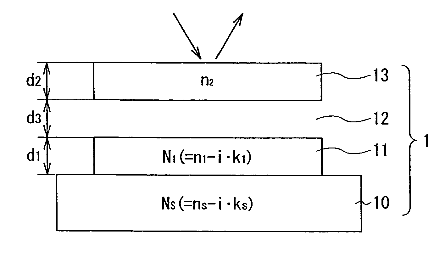
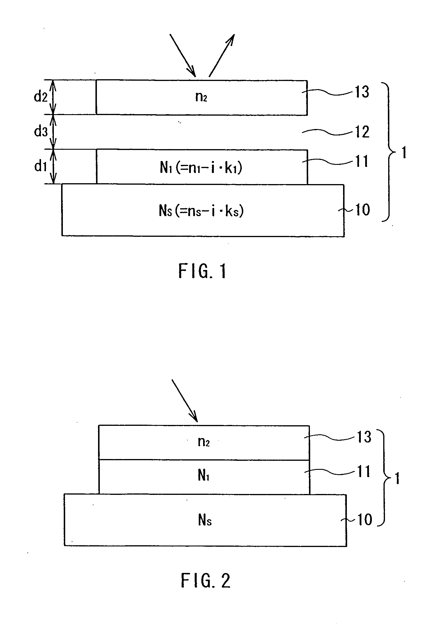
[0098]FIGS. 1 and 2 show a basic configuration of an optical multilayer structure 1 according to a first embodiment of the invention. FIG. 1 shows a high reflectance state where a gap portion 12 described hereinlater in an optical multilayer structure 1 exists. FIG. 2 is a low reflectance state where there is no gap portion 12 of the optical multilayer structure 1. The optical multilayer structure 1 is used as, concretely for example, an optical switching device. By arranging a plurality of optical switching devices one-dimensionally or two-dimensionally, an image display can be constructed. As will be described in detail hereinlater, in the case of fixing the optical multilayer structure 1 in a structure as shown in FIG. 2, it can be used as an antireflection film.
[0099] The optical multilayer structure 1 is constructed by stacking, on a substrate 10, an optical-absorbing first layer 11 in contact with the substrate 10, the gap portion 12 having a changeable size capable of causin...
concrete examples
[0126]FIG. 8 shows the relation between the wavelength (designed wavelength of 550 nm) of incident light and reflectance in the case of using an opaque carbon substrate (Ns=1.90, k=0.75) as the substrate, a Ta layer (N1=2.46, k=1.90) as the first layer 11, an air layer (n2=1.00) as the gap portion 12, and a stacked film (composite refractive index n2=2.0, k=0) of an Si3N4 film and an ITO (Indium-Tin Oxide) film as the second layer 13. (a) indicates a characteristic in the case where an optical film thickness of the gap portion (air layer) is “0” (low reflectance side) and (b) indicates a characteristic in the case where the optical film thickness is “λ / 4” (137.5 nm) (high reflectance side). FIGS. 9 and 10 are optical admittance diagrams shown as a reference. FIG. 9 shows the case of low reflectance. FIG. 10 shows the case of high reflectance.
[0127] As obviously understood from FIG. 8, in the optical multilayer structure 1 of the embodiment, when the optical film thickness of the ga...
second embodiment
[0164] Each of FIGS. 25 and 26 shows a basic configuration of an optical multilayer structure 2 according to a second embodiment of the invention. FIG. 25 shows a state where a gap portion 53 which will be described hereinlater exists in the optical multilayer structure 2, and FIG. 26 shows a state where there is no gap portion in the optical multilayer structure 2.
[0165] The optical multilayer structure 2 is constructed by stacking, on a substrate 50 made of, for example, a metal, a first transparent layer 51 made of a material having a high refractive index, a second transparent layer 52 made of a material having a low refractive index, a gap portion 53 having a changeable size capable of causing an optical interference phenomenon, and a third transparent layer 54 made of a material having a high refractive index.
[0166] The position of the gap portion 53 is not limited to the example (the position between the second and third transparent layers 52 and 54) but the gap portion 53 ...
PUM
| Property | Measurement | Unit |
|---|---|---|
| refractive index | aaaaa | aaaaa |
| refractive index | aaaaa | aaaaa |
| reflectance | aaaaa | aaaaa |
Abstract
Description
Claims
Application Information
 - R&D
- Intellectual Property
- Life Sciences
- Materials
- Tech Scout
- Unparalleled Data Quality
- Higher Quality Content
- 60% Fewer Hallucinations
Browse by: Latest US Patents, China's latest patents, Technical Efficacy Thesaurus, Application Domain, Technology Topic, Popular Technical Reports.
© 2025 PatSnap. All rights reserved.Legal|Privacy policy|Modern Slavery Act Transparency Statement|Sitemap|About US| Contact US: help@patsnap.com


