Coated article with absorbing layer
a coating article and absorbing layer technology, applied in the direction of natural mineral layered products, transportation and packaging, chemistry apparatus and processes, etc., can solve the problems of high visible transmission, many other characteristics (e.g. color, heat treatmentability, etc., being significantly altered, etc., to achieve the effect of easy and efficient adjustmen
- Summary
- Abstract
- Description
- Claims
- Application Information
AI Technical Summary
Benefits of technology
Problems solved by technology
Method used
Image
Examples
examples
[0045] The following examples are provided for purposes of example only, and are not intended to be limiting. Example processing techniques used for sputtering the Example coatings may be found in related U.S. Pat. No. 6,686,050, the disclosure of which is incorporated herein by reference.
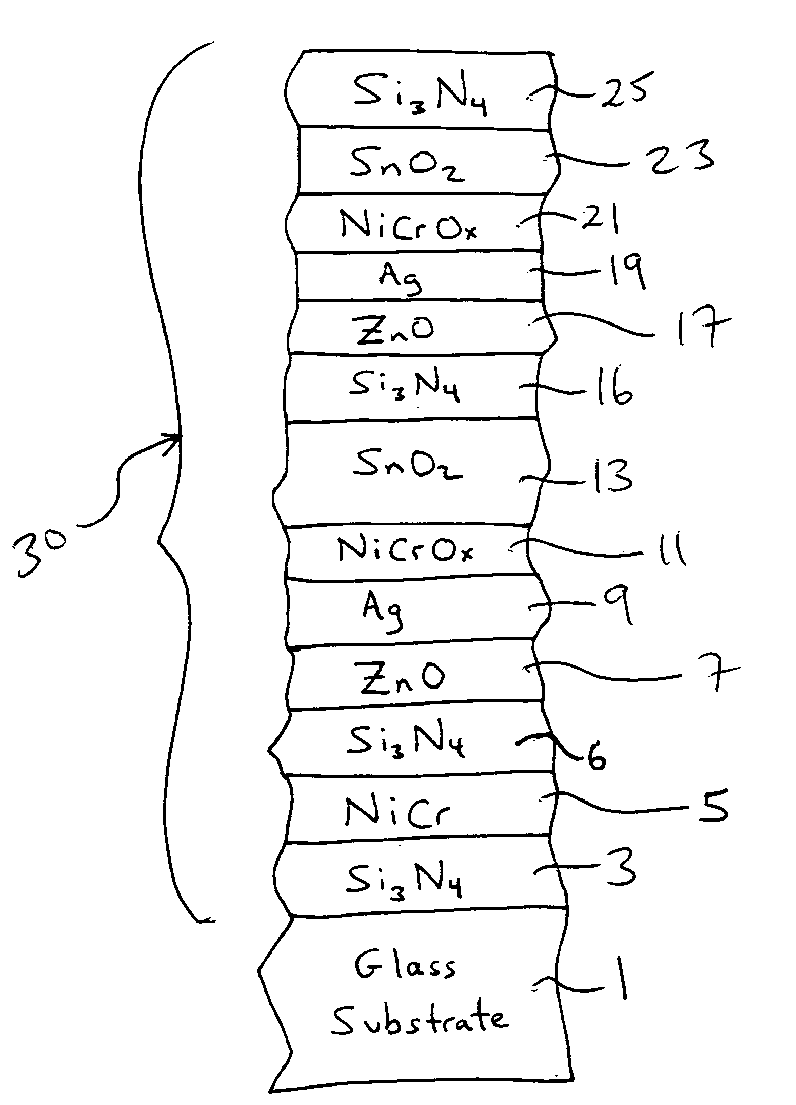
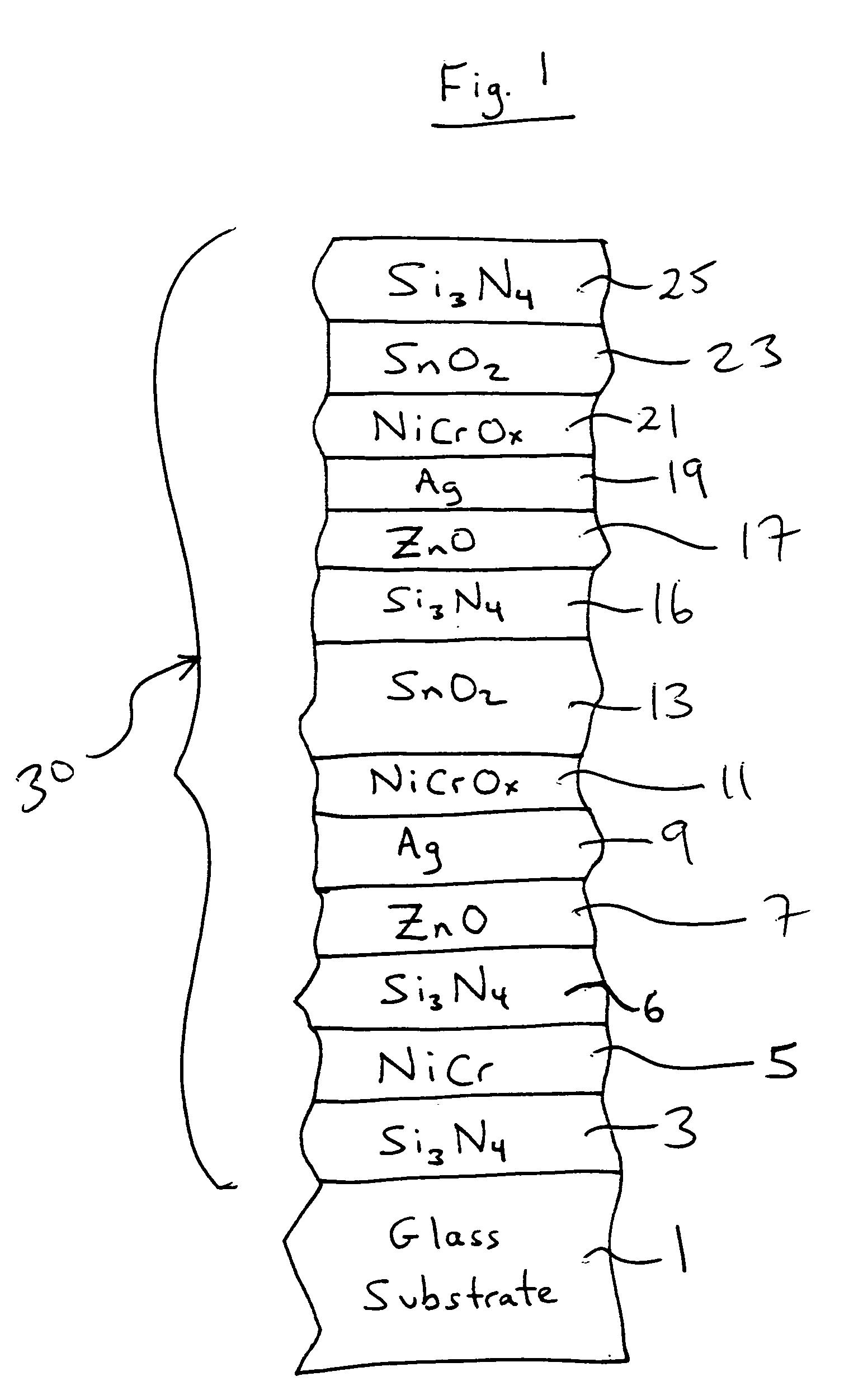
[0046] Examples 1 and 2 are in accordance with the FIG. 1 embodiment, and have the layers shown in FIG. 1 with the below listed thicknesses (layers listed from the glass substrate outwardly).
examples 1 and 2
Layer Stack
[0047]
LayerExample 1Example 2Glass SubstrateSi3N4 (layer 3)80Å80ÅNiCr (layer 5)33Å62.5ÅSi3N4 (layer 6)100Å100ÅZnO (layer 7)75Å75ÅAg (layer 9)80Å80ÅNiCrOx (layer 11)30Å30ÅSnO2 (layer 13)580Å580ÅSi3N4 (layer 16)100Å100ÅZnO (layer 17)75Å75ÅAg (layer 19)174Å174ÅNiCrOx (layer 21)30Å30ÅSnO2 (layer 23)100Å100ÅSi3N4 (layer 25)194Å194Å
[0048] It can be seen that the only difference between Examples 1 and 2 is the thickness of the absorption layer 5. In Example 1, the absorption layer 5 is 33 Å thick, whereas in Example 2 it is 62.5 ↑ thick. Examples 1 and 2 were characterized by the optical characteristics set forth below.
Optical Characteristics of Examples 1-2 (Monolithic)
[0049]
Example 1Example 2Visible Transmission (Y)(Ill. C 2 deg.):60%46%a*−4.5−5.7b*4−1.8Glass Side Reflective (RY)(Ill C, 2 deg.):13.5%10.5%a*−6−5b*−5−4.2Film Side Reflective (FY)(Ill. C, 2 deg.):7%7.5%a*−5−2.4b*2.53.3SHGC:0.290.22
[0050] It can be seen from the tables above that the increased thickness of the N...
examples 3 and 4
Layer Stack
[0054]
LayerExample 3Example 4Glass SubstrateTiO2 (layer 2)135Å135ÅSi3N4 (layer 6)100Å100ÅZnO (layer 7)75Å75ÅAg (layer 9)110Å110ÅNiCrOx (layer 11)20Å20ÅSnO2 (layer 13)660Å660ÅSi3N4 (layer 16)100Å100ÅZnO (layer 17)75Å75ÅAg (layer 19)149Å149ÅNiCr (layer 5)25Å72.5ÅSi3N4 (layer 25)245Å245Å
[0055] It can be seen that the only difference between Examples 3 and 4 is the thickness of the NiCr absorption layer 5 which is located over the top Ag layer in the double-silver stack. In Example 3, the absorption layer 5 is 25 Å thick, whereas in Example 4 it is 72.5 Å thick. Examples 3 and 4 were characterized by the optical characteristics set forth below.
Optical Characteristics of Examples 3-4 (Monolithic)
[0056]
Example 3Example 4Visible Transmission (Y)(Ill. C 2 deg.):60.4%46.2%a*−3−4b*−0.2−2Glass Side Reflective (RY)(Ill C, 2 deg.):10.5%12.5%a*−3.10.8b*−6.5−12Film Side Reflective (FY)(Ill. C, 2 deg.):17%20.1%a*−3.9−3.5b*5.210.4SHGC:0.320.25
[0057] It can be seen from the tables above...
PUM
| Property | Measurement | Unit |
|---|---|---|
| sheet resistance | aaaaa | aaaaa |
| sheet resistance | aaaaa | aaaaa |
| SHGC | aaaaa | aaaaa |
Abstract
Description
Claims
Application Information
 - R&D
- Intellectual Property
- Life Sciences
- Materials
- Tech Scout
- Unparalleled Data Quality
- Higher Quality Content
- 60% Fewer Hallucinations
Browse by: Latest US Patents, China's latest patents, Technical Efficacy Thesaurus, Application Domain, Technology Topic, Popular Technical Reports.
© 2025 PatSnap. All rights reserved.Legal|Privacy policy|Modern Slavery Act Transparency Statement|Sitemap|About US| Contact US: help@patsnap.com


