Distortion correction circuit
a technology of distortion correction and circuit, applied in the field of distortion correction circuit, can solve the problem of poor and achieve the effect of improving the distortion characteristic of inexpensive optical systems
- Summary
- Abstract
- Description
- Claims
- Application Information
AI Technical Summary
Problems solved by technology
Method used
Image
Examples
first embodiment
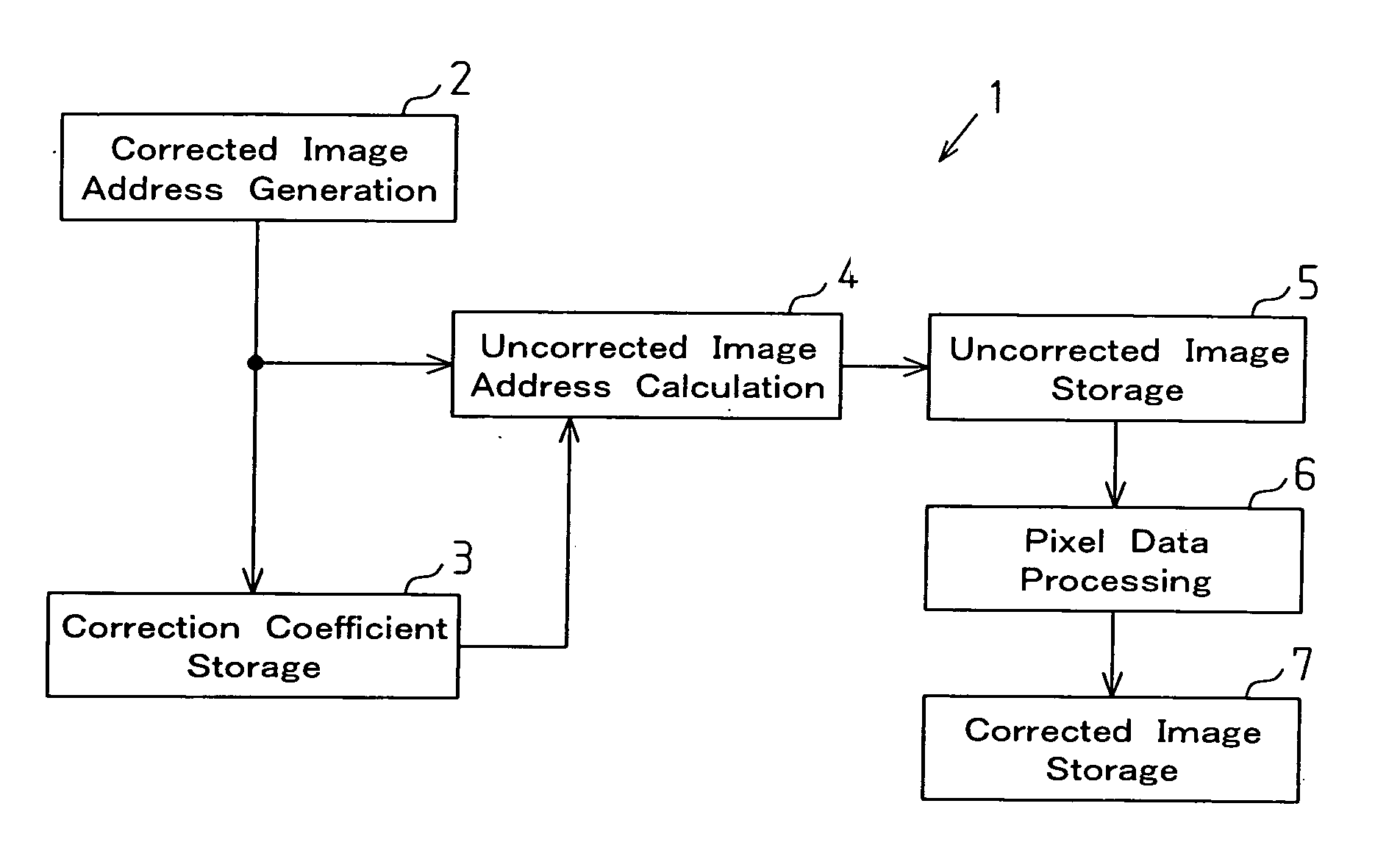
[0026] As shown in FIG. 1, a distortion correction circuit 1 according to the present invention includes a corrected image address generation circuit 2, a correction coefficient storage circuit 3, an uncorrected image address calculation circuit 4, an uncorrected image storage circuit 5, a pixel data processing circuit 6, and a corrected image storage circuit 7. In the distortion correction circuit 1, the corrected image address generation circuit 2 generates a horizontal address and a vertical address for each pixel of a corrected image. The uncorrected image address calculation circuit 4 reads a pixel pitch correction coefficient, which is associated with the horizontal and vertical addresses generated by the corrected image address generation circuit 2, from the correction coefficient storage circuit 3. The uncorrected image address calculation circuit 4 calculates the data addresses of an uncorrected image using the horizontal and vertical addresses and the pixel pitch correctio...
second embodiment
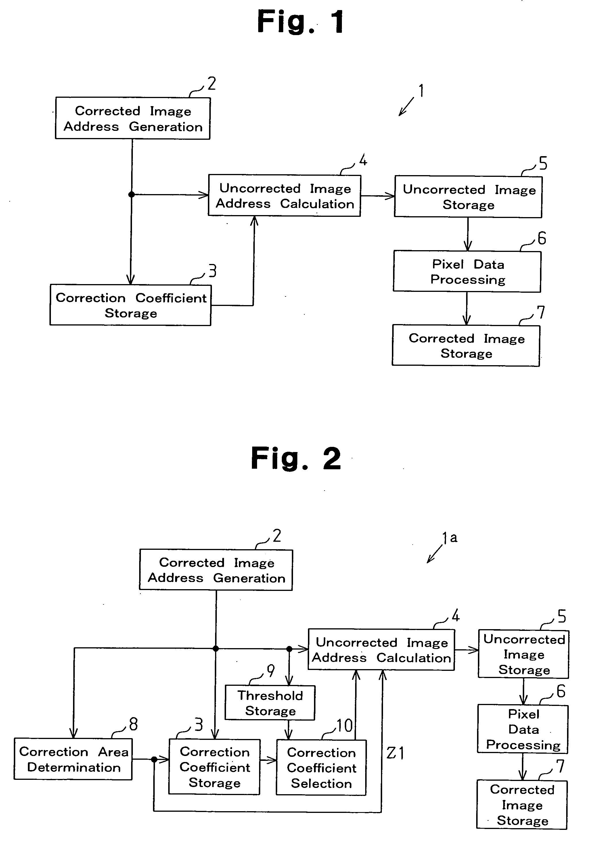
[0029] As shown in FIG. 2, a distortion correction circuit 1a according to the present invention includes a corrected image address generation circuit 2, a correction coefficient storage circuit 3, an uncorrected image address calculation circuit 4, an uncorrected image storage circuit 5, a pixel data processing circuit 6, a corrected image storage circuit 7, and a correction area determination circuit 8. The correction area determination circuit 8 determines whether the horizontal and vertical addresses generated by the corrected image address generation circuit 2 are in an area that requires correction or in an area that requires no correction. When these addresses are in an area that requires no correction, the correction area determination circuit 8 outputs a no-correction signal Z1. When receiving the no-correction signal Z1, the uncorrected image address calculation circuit 4 uses the horizontal and vertical addresses generated by the corrected image address generation circuit...
third embodiment
[0032] The following describes a distortion correction circuit according to the present invention.
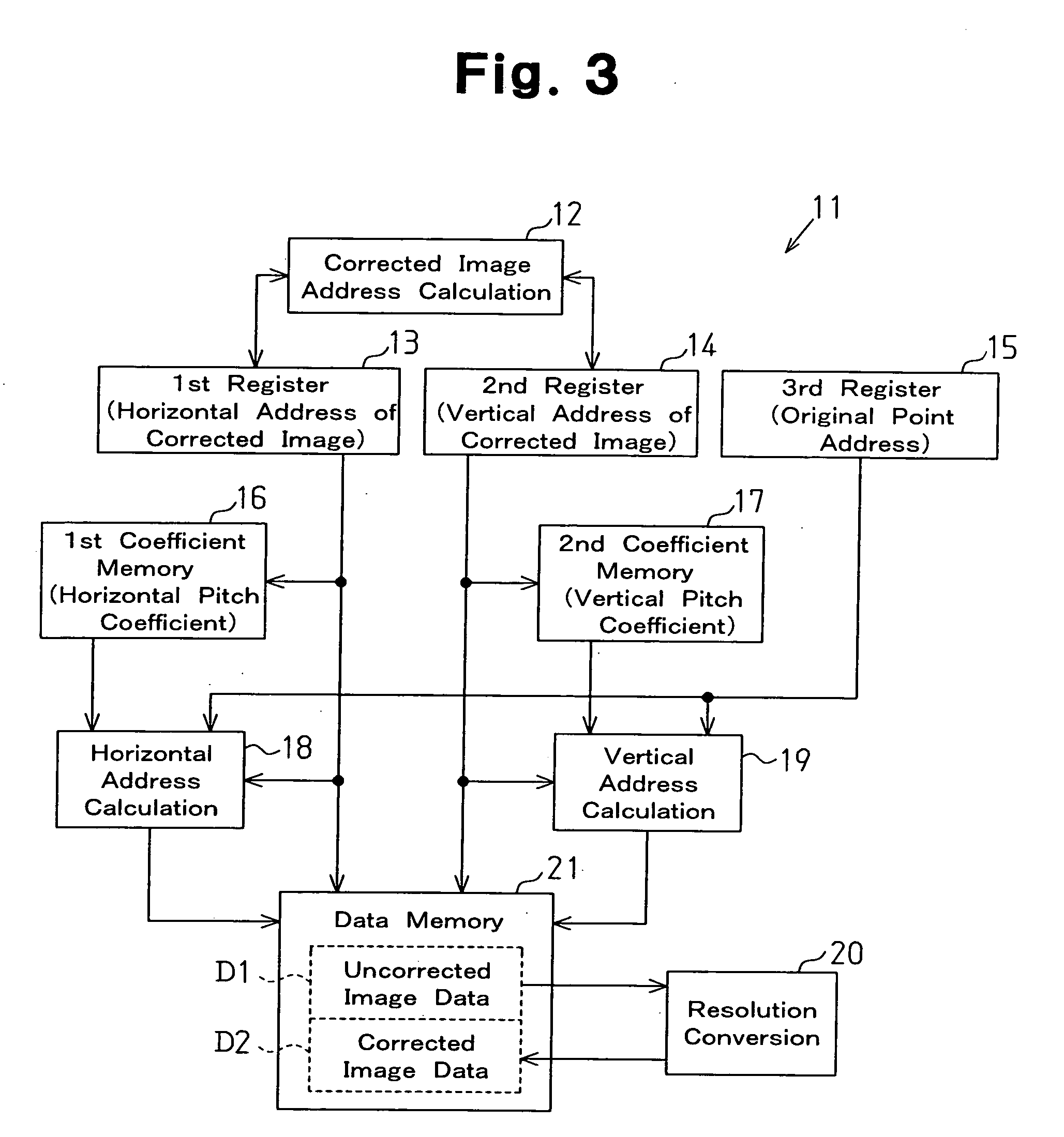
[0033] As shown in FIG. 3, a distortion correction circuit 11 according to the third embodiment is used for a digital camera, and processes data for an uncorrected image formed by an imaging device (e.g., a CCD sensor and a CMOS sensor) of the digital camera, to generate a corrected image whose distortion has been corrected. The corrected image generated by the distortion correction circuit 11 is, for example, a square image with a size of 4096×4096 pixels. To generate the corrected image, the distortion correction circuit 11 searches an uncorrected image (original image) for image data for a horizontal address and a vertical address of each pixel of the corrected image. The original image is larger than the corrected image. The original image is, for example, an image with the size of (4096+α)×(4096+α) pixels including pincushion distortion as shown in FIG. 4.
[0034] As shown in FIG. 3...
PUM
 Abstract
Description
Claims
Application Information
 - R&D
- Intellectual Property
- Life Sciences
- Materials
- Tech Scout
- Unparalleled Data Quality
- Higher Quality Content
- 60% Fewer Hallucinations
Browse by: Latest US Patents, China's latest patents, Technical Efficacy Thesaurus, Application Domain, Technology Topic, Popular Technical Reports.
© 2025 PatSnap. All rights reserved.Legal|Privacy policy|Modern Slavery Act Transparency Statement|Sitemap|About US| Contact US: help@patsnap.com


