
Organic electro luminescence device and fabrication method thereof

Active Publication Date: 2005-06-30
LG DISPLAY CO LTD
View PDF14 Cites 26 Cited by
  • Summary
  • Abstract
  • Description
  • Claims
  • Application Information

AI Technical Summary

Benefits of technology

[0014] An advantage of the present invention is to provide an organic electro luminescence device and a fabrication method thereof in which when an organic electro luminescence layer is formed in a display area by an inkjet printing method, the organic electro luminescence layer has a uniform thickness irrespective of a position of the organic electro luminescence layer in the display area, which results in a uniform luminance and a good quality of picture.

Problems solved by technology

However, since the LCD devices are a light receiving device, not a light emitting device, and have disadvantages in brightness, contrast, viewing angle, large-size area and the like, a new flat panel display device is being actively developed in order to overcome such disadvantages of the LCD devices.
However, the passive matrix OEL devices have many limitations in resolution, power consumption, life expectancy and the like.
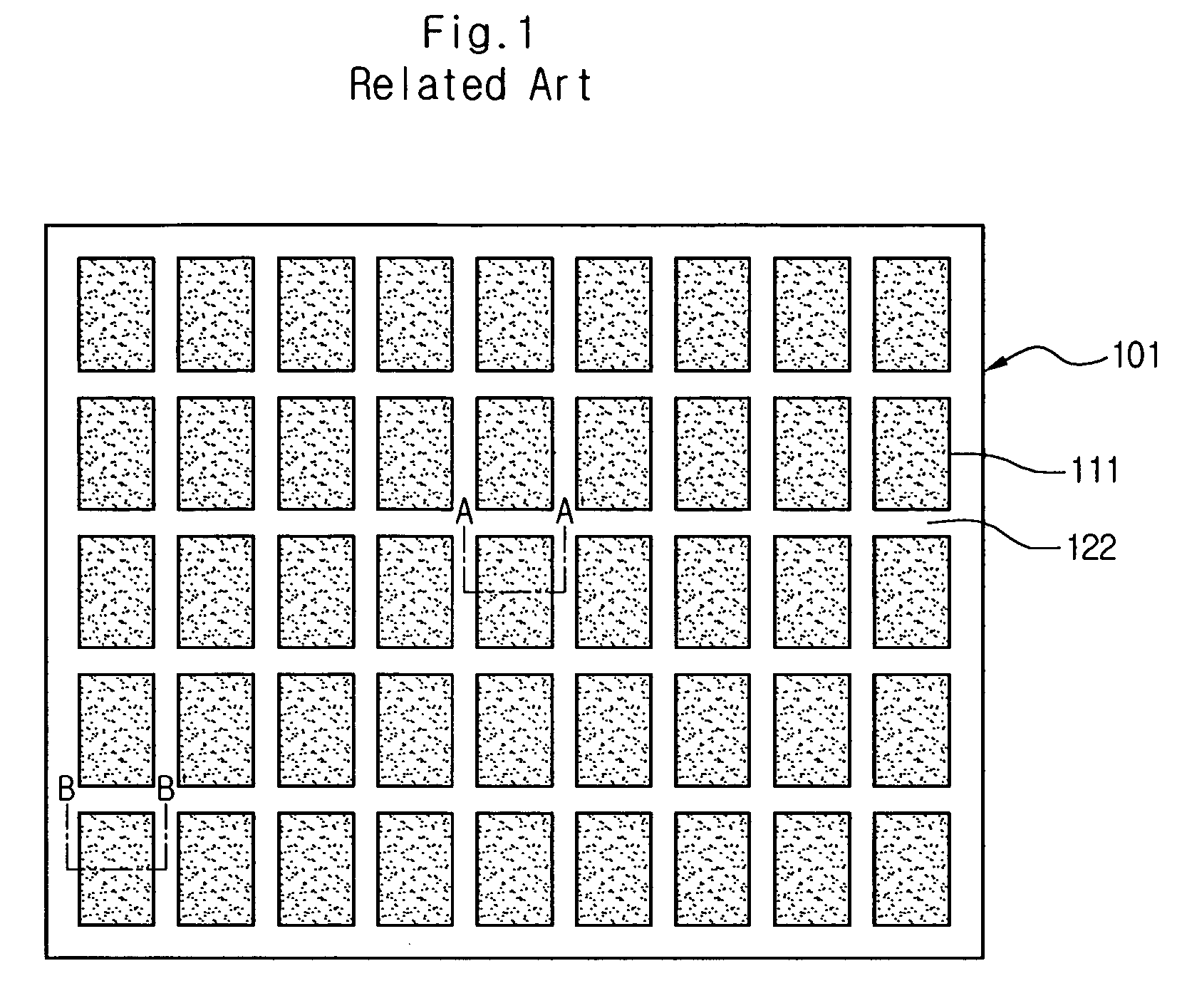
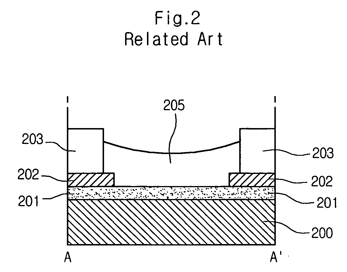
However, as shown in FIG. 3, the organic electro luminescence layer at an edge portion of the display area dries unevenly due to a concentration difference of the solvent molecules.
The unevenness of the organic electro luminescence layer causes luminance irregularity, leading to display failure and product failure.

Method used


Image

  • Organic electro luminescence device and fabrication method thereof
  • Organic electro luminescence device and fabrication method thereof
  • Organic electro luminescence device and fabrication method thereof

Examples


Embodiment Construction

[0027] Reference will now be made in detail to an embodiment of the present invention, example of which is illustrated in the accompanying drawings. Wherever possible, the same reference numbers will be used throughout the drawings to refer to the same or like parts.

[0028]FIG. 4 is a schematic plan view illustrating a panel of an organic electro luminescence device according to an embodiment of the present invention.

[0029] As shown in FIG. 4, the organic electro luminescence device according to the present invention includes a display area 310 having a plurality of display pixels 311 and a dummy area 350 having a plurality of dummy pixels 351 and formed at a periphery of the display area 310.

[0030] Each of the display pixels 311 and the dummy pixels 351 has a bank structure with a barrier 322. The barrier 322 prevents an organic electro luminescence material from being diffused from a luminescence area to a non-luminescence area. The organic electro luminescence material is forme...


PUM


Abstract

Disclosed is an organic electro luminescence device having a display area and a dummy area, the display area having a plurality of display pixels for displaying an image, and the dummy area having a plurality of dummy pixels and being provided at a periphery of the display area, an anode at the display area on a substrate; a buffer layer on the anode of the display area and on the substrate of the dummy area; a barrier on the buffer layer for partitioning the display pixels and the dummy pixels on the substrate and; an organic electro luminescence layer in the display and dummy pixels.

Description

[0001] This application claims the benefit of Korean Patent Application No. 2003-100631, filed on Dec. 30, 2003, which is hereby incorporated by reference for all purposes as if fully set forth herein. BACKGROUND OF THE INVENTION [0002] 1. Field of the Invention [0003] The present invention relates to an organic electro luminescence device and a method of fabrication thereof. [0004] 2. Discussion of the Related Art [0005] As large-size display devices are in demand, flat panel display (FPD) devices, which occupy less space than conventional displays, are increasingly required. Until now, liquid crystal display (LCD) devices are most highlighted due to their low-power consumption and light weight. However, since the LCD devices are a light receiving device, not a light emitting device, and have disadvantages in brightness, contrast, viewing angle, large-size area and the like, a new flat panel display device is being actively developed in order to overcome such disadvantages of the L...

Claims


Application Information

Patent Timeline
IPC IPC(8): H01J1/62H01J63/04H05B33/10H01L27/32H01L51/00H05B33/12H05B33/22H05B33/26
CPCH01L27/3223H01L51/0005H01L27/3246H10K59/88H10K71/135H10K59/122H05B33/10
Inventor LEE, JAE YOONKIM, KWAN SOO
Owner LG DISPLAY CO LTD
Learn More