Semiconductor device

Active Publication Date: 2005-06-23
RENESAS ELECTRONICS CORP
View PDF6 Cites 28 Cited by
  • Summary
  • Abstract
  • Description
  • Claims
  • Application Information

AI Technical Summary

Benefits of technology

[0017] It is an object of the present invention to provide a semiconductor device which can be miniaturized, does not require a special step at the time of fabrication and shows a sufficient protection performance even against a negative ESD current.
[0019] According to the invention, the first contact, the second conductivity type diffusion layer, the second contact, the wire and the third contact are coupled in series between the pad and the one of the source and drain. When a positive ESD current is supplied to the pad, therefore, a contact resistance can be added between the pad and the other one of the source and the drain while keeping the substantial element length to be discussed later small as compared with those in the prior arts. When a negative ESD current is supplied to the pad, the current flows in the current path which is formed by the top surface of the semiconductor substrate, the second conductivity type diffusion layer and the first contact, so that the resistance of the current path is low. Further, the first to third contacts can be formed in the normal contact fabrication process and do not require a special step.
[0020] It is preferable that a direction from the first contact toward the second contact is a widthwise direction of a gate of the second conductivity type transistor. The widthwise direction of the gate is a direction orthogonal to the direction from the source toward the drain. Accordingly, the current path in the second conductivity type diffusion layer runs in the direction orthogonal to the direction from the source to the drain, so that the ballast resistor can be added with the diffusion layer resistor without increasing the distance between the source and region. Because individual fingers can be arranged close to one another as will be discussed later, the substrate coupling effect becomes greater and the resistance of the ballast resistor can be made relatively lower.
[0021] The semiconductor device may further include an integrated circuit portion coupled to the pad in parallel to the second conductivity type transistor. And when an electrostatic discharge current is input to the pad, the second conductivity type transistor allows the electrostatic discharge current to flow. This can protect the integrated circuit portion against ESD. At this time, the pad may also serve as the output pad of the integrated circuit portion or may serve as an input pad. The pad may be a power supply pad of the integrated circuit portion.
[0025] The semiconductor device may further include: another second conductivity type diffusion layer formed at a position insulated from the second conductivity type transistor and the second conductivity type diffusion layer at the top surface of the semiconductor substrate; another wire; a fourth contact which couples a pad to the another second conductivity type diffusion layer; and a fifth contact which couples the another second conductivity type diffusion layer to the another wire. And, the first contact couples the another wire to the second conductivity type diffusion layer for coupling the pad to the second conductivity type diffusion layer. This can make the resistance to be added to the other one of the source and the drain higher.
[0029] According to the invention, the first to third contacts and the second conductivity type diffusion layer are coupled between the pad and one of the source and drain, so that a ballast resistance using the contact resistance can be added between the pad and one of the source and the drain. When a second conductivity type transistor is used as the ESD protecting element, therefore, it is possible to acquire an ESD protecting element whose substantial element length is small, and which has a small layout area required and a high protection performance even against a negative ESD current, without involving a special step.

Problems solved by technology

In this case, however, a problem would arise.
The prior arts however have the following problems.
This makes it difficult to control the horizontal shape precisely and stands in the way of designing the element compact.
When a negative ESD current is supplied to the pad 131, however, the ESD protecting element does not snap back, no ballast resistor is required, and the ballast resistor, if present, would reduce the protection performance.
In other words, the conventional ESD protecting element has a low protection performance against a negative ESD current.

Method used


Image

  • Semiconductor device
  • Semiconductor device
  • Semiconductor device

Examples


first embodiment

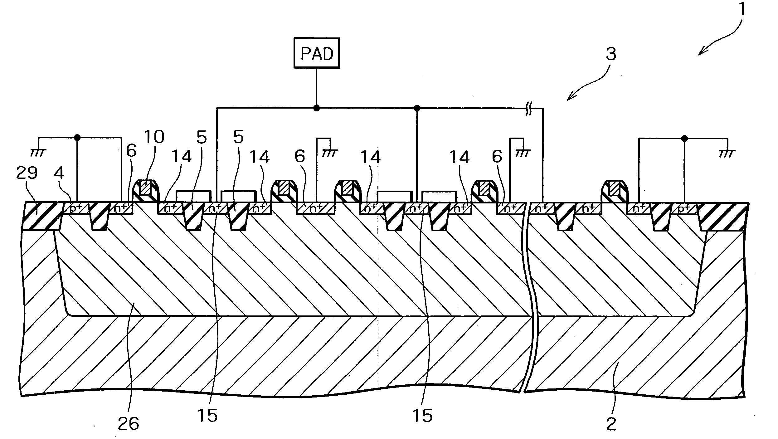
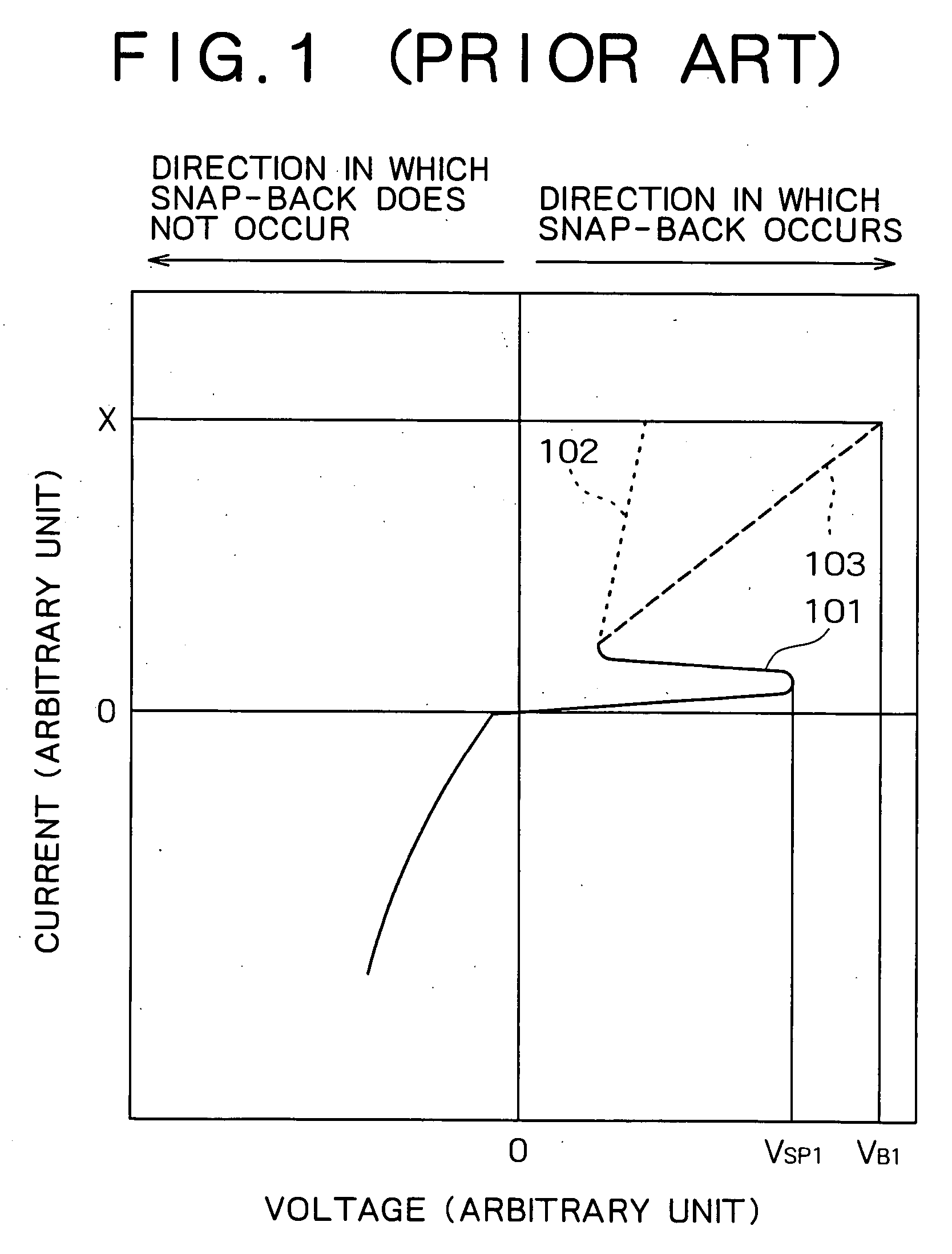
[0050] Preferred embodiments of the present invention will be specifically described below with reference to the accompanying drawings. To begin with the invention will be discussed. FIG. 4 is a plan view exemplarily illustrating the principle of the embodiment. FIG. 5 is a cross-sectional view showing a part of a semiconductor device according to the embodiment. FIG. 6 is a plan view showing an ESD protecting element in the semiconductor device according to the embodiment. FIG. 7 is a plan view showing a part of the ESD protecting element shown in FIG. 6. FIG. 8 is a perspective view showing a part of the ESD protecting element shown in FIG. 7. FIGS. 4 and 5 illustrate only the typical components of the semiconductor device of the embodiment with the other components omitted from the illustrations.

[0051] As shown in FIG. 4, the key point of the embodiment lies in that the semiconductor device, which has a first conductivity type region 301 formed at the top surface of a semiconduct...

fourth embodiment

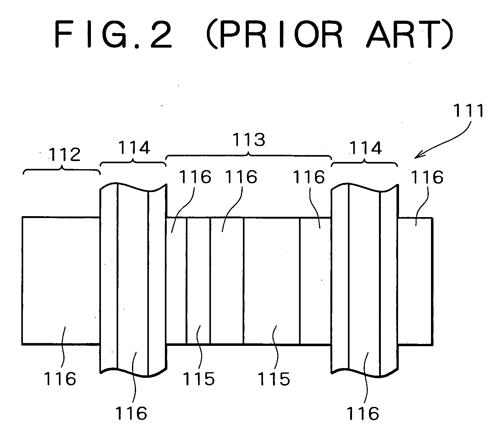
[0087] the invention will be described next. FIG. 15 is a plan view showing an ESD protecting element according to the embodiment. As shown in FIG. 15, in the embodiment, the n+ type diffusion region 15 is separated into four n+ type diffusion regions, two n+ type diffusion regions 15b and two n+ type diffusion regions 15c, in the direction 12 in the ballast resistor region 7. In each ballast resistor region 7, the n+ type diffusion regions 15b and 15c are laid out in the order of the n+ type diffusion region 15b, the n+ type diffusion region 15c, the n+ type diffusion region 15c and the n+ type diffusion region 15b. The STI region 5 is formed between the n+ type diffusion regions 15b and 15c. The metal wire 20 is separated into two metal wires 20a in the direction 12, and the metal wire 22 is separated into two metal wires 22a in the direction 12, with a wire 25 provided between the metal wires 20a.

[0088] The contact 19a is provided at the n+ type diffusion region 15b at a positio...


PUM


Abstract

In an ESD protecting element, a plurality of source regions and a plurality of ballast resistor regions are formed. A drain region is formed at a region which is in contact with a channel region in the ballast resistor region, and an n+ type diffusion region is formed at a region isolated from the drain region via an STI region. A third contact is provided on the drain region, first and second contacts are formed on the n+ type diffusion region, and the first contact is connected to a pad. The second contact is coupled to the third contact by a metal wire. The first and second contacts are laid out along the widthwise direction of a gate.

Description

BACKGROUND OF THE INVENTION [0001] 1. Field of the Invention [0002] The present invention relates to a semiconductor device having an ESD (Electro Static Discharge) protecting element. The invention can be applied to a semiconductor device which needs a constant resistance in a limited area, and can be suitably applied to, particularly, a case where the ballast resistance of the ESD protecting element is provided. [0003] 2. Description of The Related Art [0004] With the recent enhancement of the functions and the performance of semiconductor devices, there is a demand for multi-pin semiconductor devices which have over several thousand I / O (Input / Output) pins. Accordingly, the area of a single I / O block considerably influences the downsizing and cost reduction of the overall semiconductor device. Elements which have a large ratio of occupying the area of the I / O block are an ESD protecting element and a driver element of high drive power. A multi-finger type protecting element which...

Claims


Application Information

Patent Timeline
IPC IPC(8): H01L27/04H01L21/822H01L21/8238H01L27/02H01L27/06H01L27/092
CPCH01L27/0288
Inventor OKUSHIMA, MOTOTSUGU
Owner RENESAS ELECTRONICS CORP
Why Eureka
Try Eureka