Sputtering apparatus and sputter film deposition method

a sputtering apparatus and film deposition technology, applied in the direction of instruments, optical elements, vacuum evaporation coating, etc., can solve the problems of low productivity, significant productivity reduction, and difficult control of conventional film deposition apparatuses, and achieve high precision and rapid film deposition and film thickness control.

Inactive Publication Date: 2005-06-09
ASAHI GLASS CO LTD
View PDF13 Cites 11 Cited by
  • Summary
  • Abstract
  • Description
  • Claims
  • Application Information

AI Technical Summary

Benefits of technology

[0015] The AC magnetron sputtering source can perform more rapid film deposition than the magnetron sputtering source with a target mounted on a single magnetron unit. In accordance with the present invention, these two kinds of sputtering sources are combined to realize rapid and high precision film deposition.
[0042] As another mode of the present invention, according to a nineteenth aspect of the present invention, the target has a target surface inclined at such an inclination angle that when the target is located in a positional relationship to confront the substrate, the target surface is prevented from being parallel with a surface of the substrate.

Problems solved by technology

However, the conventional film deposition apparatuses have been difficult to control film thicknesses with high precision.
The conventional film deposition apparatuses have caused a problem that productivity is significantly decreased since the film deposition rate needs to be lowered in order to increase the precision of film thicknesses.
This method is disadvantageous in that productivity is low since film deposition processes and measuring processes are alternately performed and since film deposition is interrupted during measurement.
However, it is not easy to make each of the film thicknesses uniform since it is difficult to equalize the conditions of both cathodes.

Method used


Image

  • Sputtering apparatus and sputter film deposition method
  • Sputtering apparatus and sputter film deposition method
  • Sputtering apparatus and sputter film deposition method

Examples


Embodiment Construction

[0088] Now, preferred embodiments of the sputtering apparatus and the sputter film deposition method according to the present invention will be described, referring to the accompanying drawings.

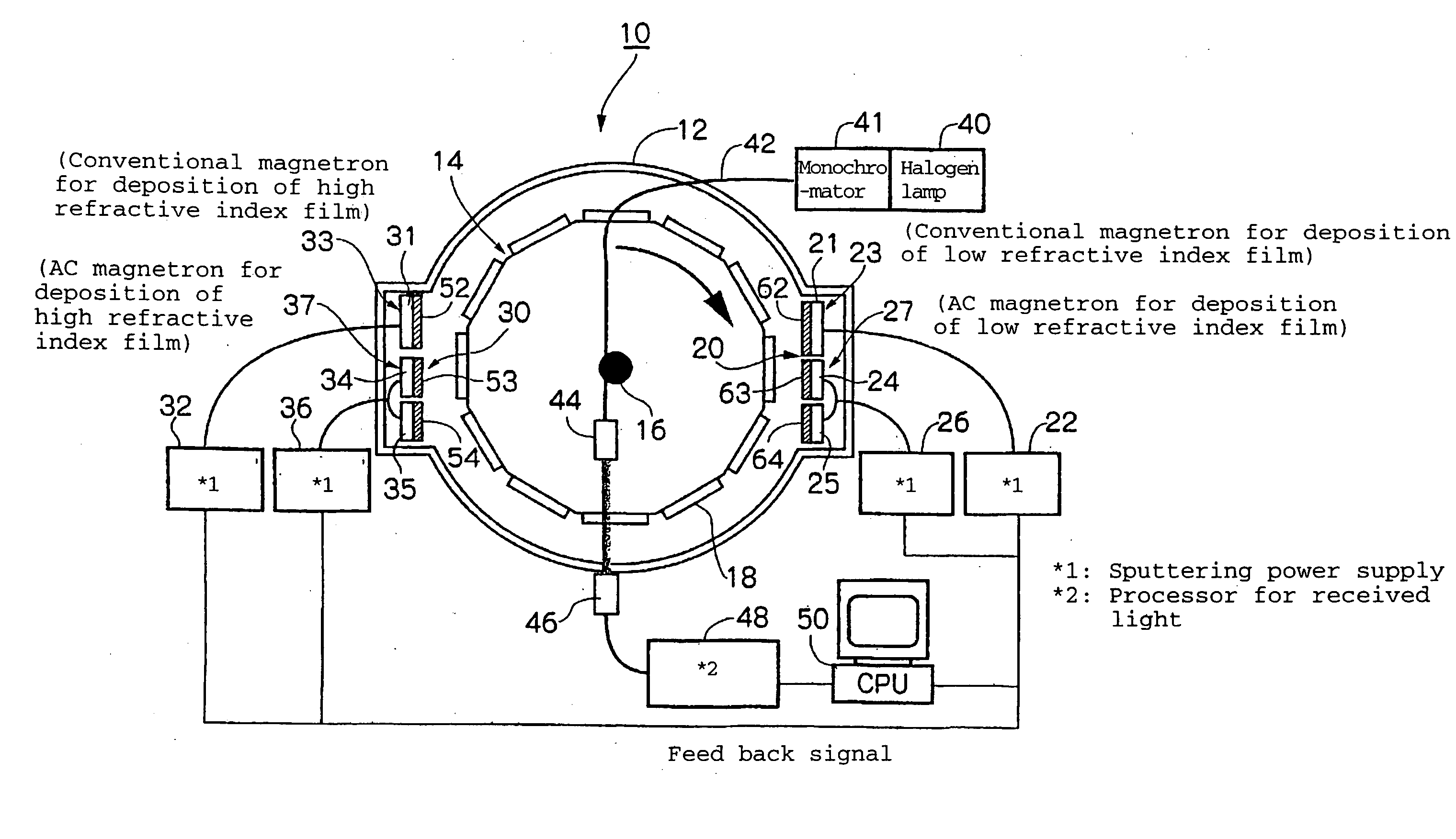
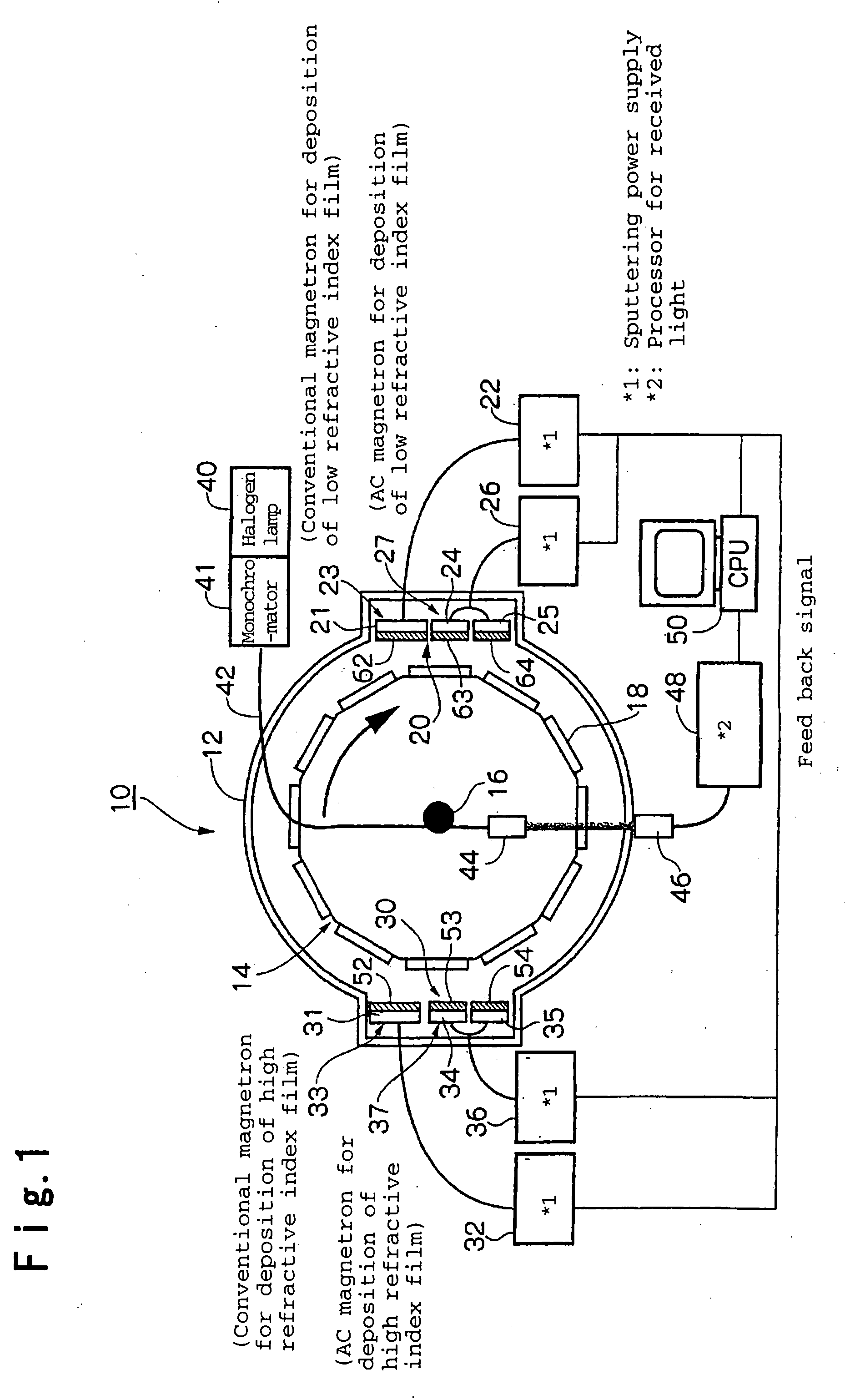
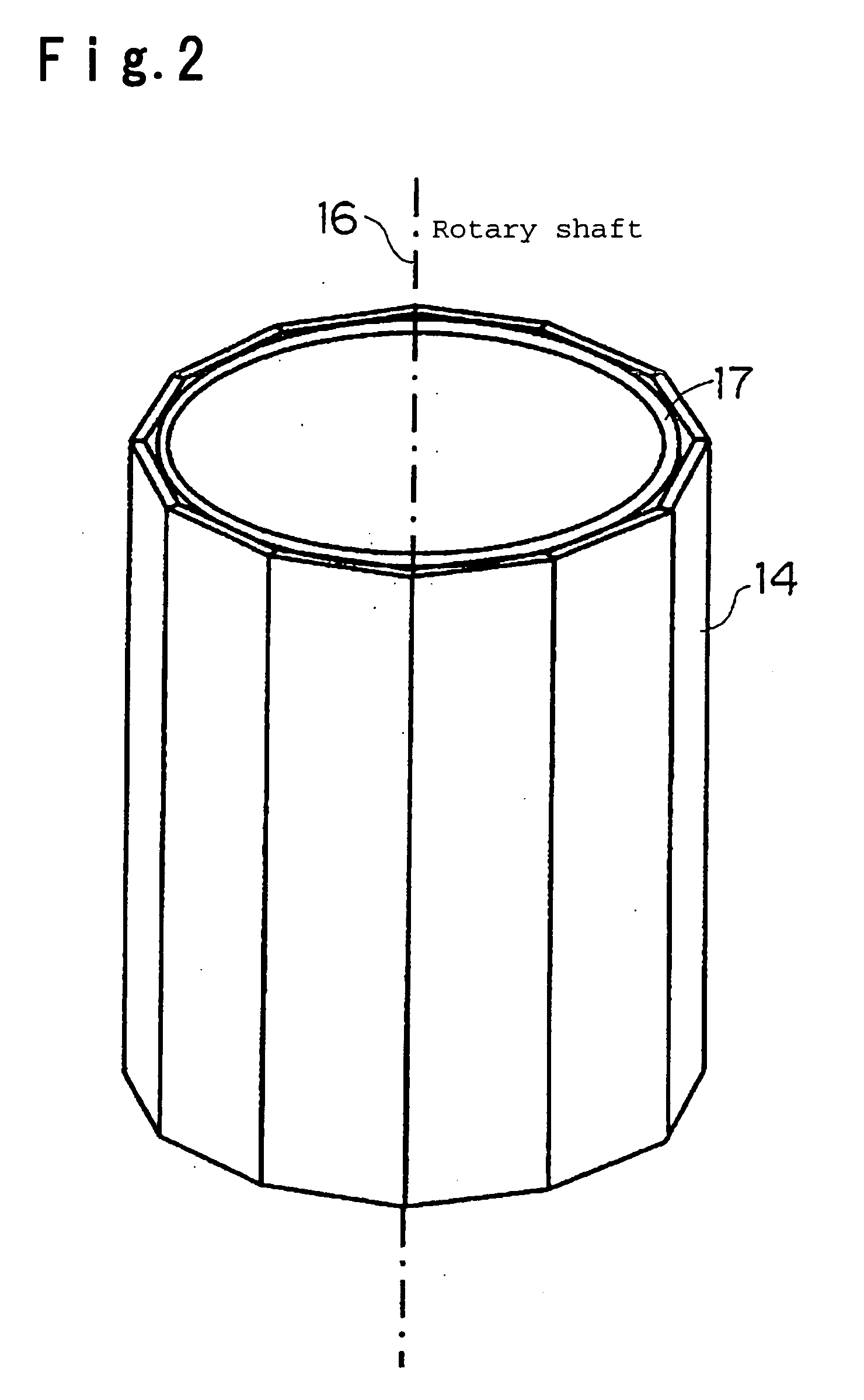
[0089]FIG. 1 is a schematic plan view showing the structure of the sputtering apparatus for depositing a multilayer optical film, according to an embodiment of the present invention, and FIG. 2 is a perspective view of substrate holders used in the apparatus. The sputtering apparatus 10 shown in FIG. 1 is a carousel type sputtering apparatus, which is configured to include a drum (not shown in FIG. 1 and indicated by reference numeral 17 in FIG. 2) and the substrate holders 14 provided on an outer peripheral surface of the drum 17 in a cylindrical chamber 12 having a height of 1.5 m and a diameter of 1.5 m, wherein the substrate holders 14 are combined in a regular dodecagonal shape having a diameter of 1 m and are supported so as to be rotatable about a central shaft 16 as the center of rot...


PUM

PropertyMeasurementUnit
incident angleaaaaaaaaaa
wavelengthaaaaaaaaaa

Abstract

A sputtering apparatus and a sputter film deposition method, which includes a conventional magnetron and an AC magnetron for deposition of a low refractive index film, and a conventional magnetron and an AC magnetron for deposition of a high refractive index film, performs film deposition by each of the AC magnetrons until having achieved 90% of a designed film thickness, and then performs the film deposition only by each of the conventional magnetrons, and which can control the film thickness with high precision and have excellent productivity.

Description

TECHNICAL FIELD [0001] The present invention relates to a sputtering apparatus and a sputter film deposition method, which are applicable to a film deposition process for, e.g., an optical filter, in particular, a sputtering apparatus and a sputter film deposition method, which are appropriate for production of a WDM filter for used in a WDM (wavelength Division Multiplexing) technique. BACKGROUND ART [0002] JP-A-3-253568 has disclosed a carousel-type sputtering apparatus for depositing a film on a substrate, such as a glass substrate. The carousel-type sputtering apparatus is a rotary batch-type sputtering apparatus, which is configured so that a substrate holder (rotary drum) formed in a polygonal and cylindrical shape are included in a chamber, and magnetrons with rectangular targets held therein are provided inside the chamber. Film deposition is performed by supplying the magnetrons with power to generate plasma on outer surfaces of the targets while rotating the substrate hold...

Claims


Application Information

Patent Timeline
Patent Type & Authority Applications(United States)
IPC IPC(8): C23C14/35C23C14/50C23C14/54C23C14/56G02B1/10H01J37/34
CPCC23C14/352C23C14/505C23C14/547H01J37/3405G02B1/10H01J37/32779C23C14/568
Inventor SHIDOJI, EIJIANDO, EIICHIYAMADA, TOMOHIROMASHIMO, TAKAHIRO
Owner ASAHI GLASS CO LTD
Why Eureka
Try Eureka