Device and data processing method employing the device

Inactive Publication Date: 2005-05-19
HITACHI LTD
View PDF5 Cites 24 Cited by
  • Summary
  • Abstract
  • Description
  • Claims
  • Application Information

AI Technical Summary

Benefits of technology

[0011] An object of the present invention is to solve the above described first to third problems and to realize an element which is able to maintain states, change functions during operation, and exhibits optimal switching property, i.e., the element has a very small resistance of several Ω or less in an on-state, and an infinite resistance in an off-state.
[0012] Another object of the present invention is to realize an LSI configuration in which functions of circuit blocks can be changed by use of bistable MEMS switches, by providing structural improvements of a MEMS switch which are necessary for employing as a bistable MEMS switch for changing LSI functions.
[0035] According to the present invention, an element in which functions are changed during operation by use of bistable MEMS switches is realized, therefore a device having a high degree of freedom for changing functions, particularly, as a representative example, a semiconductor device is realized.

Problems solved by technology

Secondly, due to the large resistance, MOS switches cannot be arranged in small switching units for changing functions.
Therefore, application to a system in which functions are changed by fine parts (small logic units), for example, cellular automata, and a large function is realized by the collections of the parts; is not possible.
Even if the application is possible, the speed will be very slow, and the device will be no more than an experimental system for confirming the principles.
Therefore, aimed effects cannot be attained.

Method used


Image

  • Device and data processing method employing the device
  • Device and data processing method employing the device
  • Device and data processing method employing the device

Examples


Embodiment Construction

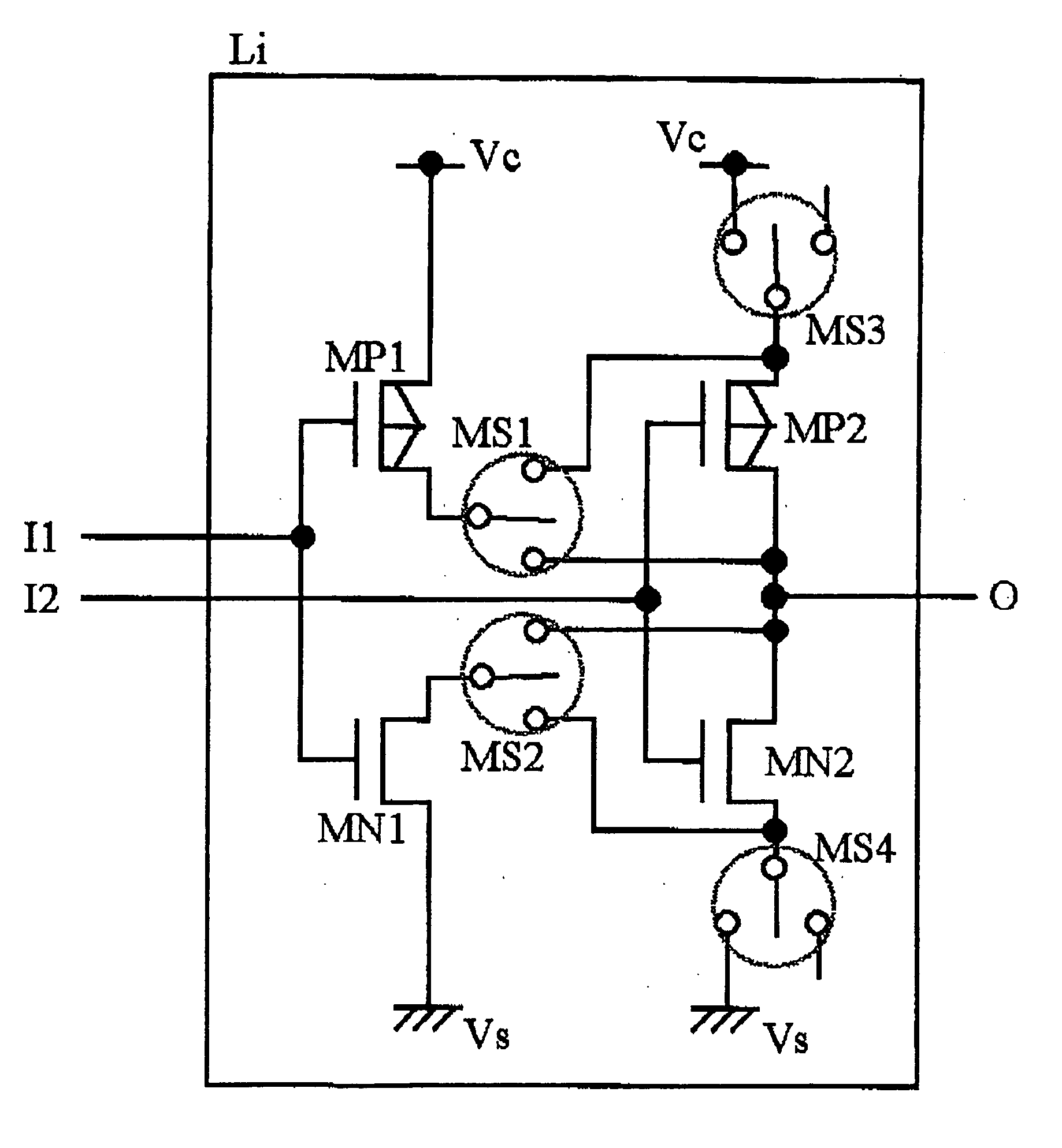
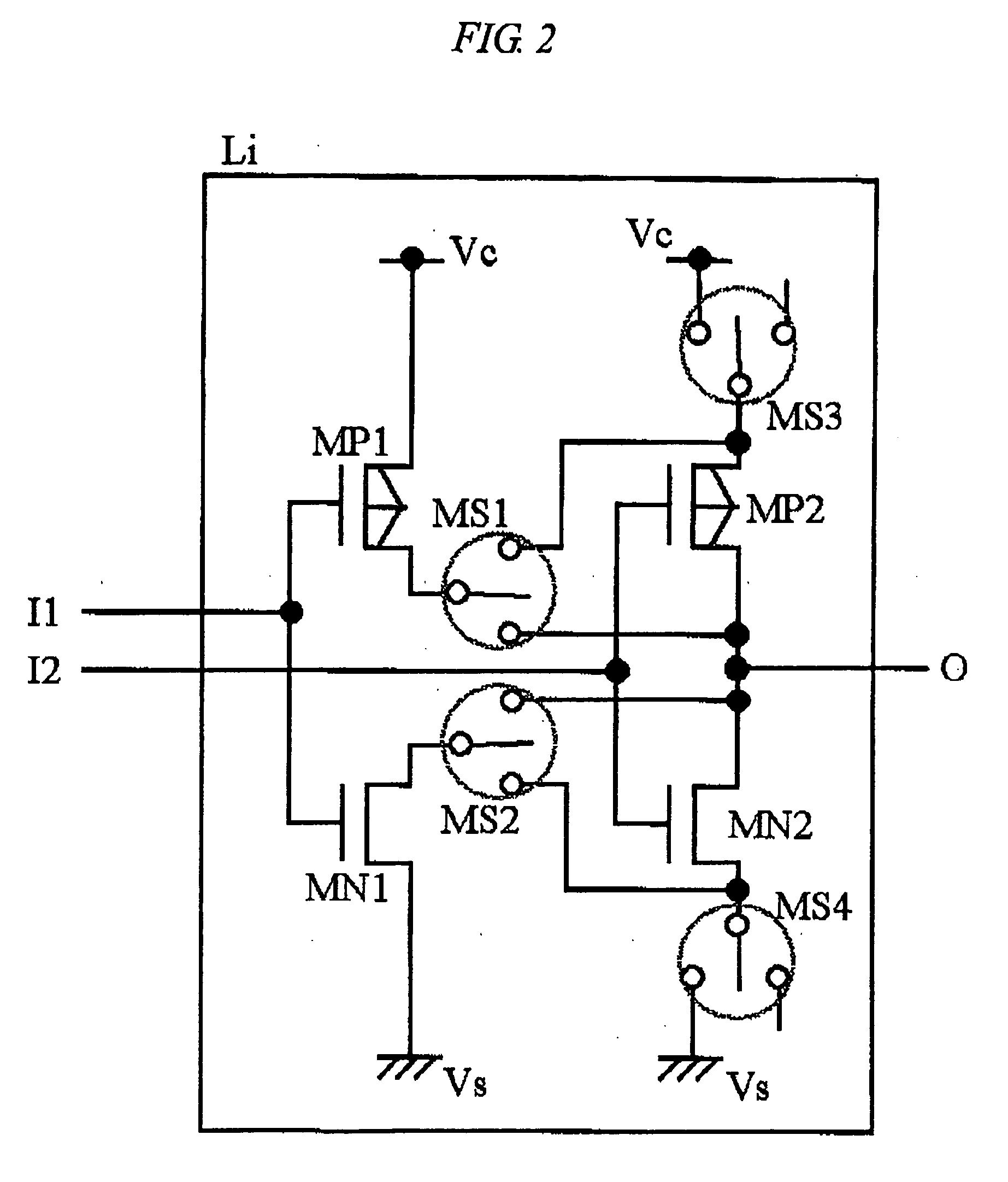
[0085] Best modes of the present invention will be explained with reference to drawings. Herein, the following technical means will next be explained as embodiments: technical means for changing functions in a logic basic element (e.g., NAND element and NOR element) level; technical means for changing a new function which is realized by combination of logic elements having certain functions; and technical means in which the function change is performed not only by direct orders from outside but also autonomically for obtaining desired output from input data.

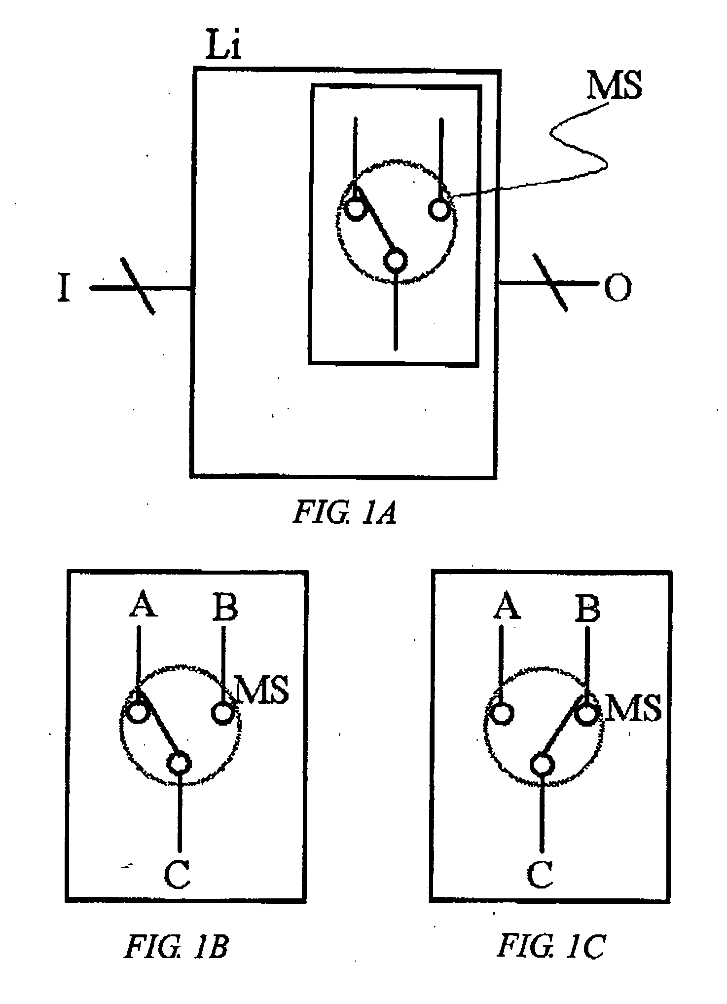
[0086]FIG. 1 is a diagram showing a means of the present invention for changing functions. In FIG. 1A, Li is a function circuit block, and I is the input and O is the output thereof. The Li can be used for plural functions by switching. For this purpose, at least a switch is required and MS serves as the switch. In the present invention, the switch is a bistable MEMS switch which employs MEMS structure (therefore, exhibiting opt...


PUM


Abstract

The present invention relates to an LSI in which functions can be changed, and realizes, particularly, a system LSI in which functions are changed by changing connections of the circuit by use of MEMS switches. A bistable MEMS switch which can maintain states, and exhibits optimal stitching property, i.e., the switch has a very small resistance of several Ω or less in an on-state, and has an infinite resistance in an off-state; is employed. An element in which functions can be changed during operation, is produced by utilizing a wiring layer of a CMOS semiconductor to form the MEMS switch. A semiconductor device exhibiting high-degree of freedom for changing functions, high-speed, and having small area, is realized.

Description

CROSS-REFERENCE TO RELATED APPLICATION [0001] The present application claims priority from Japanese Patent Application No. JP 2003-387359 filed on Nov. 18, 2003, the content of which is hereby incorporated by reference into this application. TECHNICAL FIELD OF THE INVENTION [0002] The present invention relates to a large scale integration circuit (LSI) in which functions thereof are changeable, particularly to an LSI in which functions thereof are changeable by changing the connections in the circuit by employing a mechanical element switch (a typical example is a MEMS (Micro-Electro-Mechanical Systems) switch), and also relates to a data processing method employing the LSI. BACKGROUND OF THE INVENTION [0003] Conventionally, there has been an art in which a computing circuit is composed by employing a variable logic unit, for example, that known as FPGA (Field Programmable Gate Array) or FPLD (Field Programmable Logic Device) (for example, see Japanese Patent Application Laid-Open P...

Claims


Application Information

Patent Timeline
IPC IPC(8): H01L21/82H01L21/822H01L27/04H03K19/173H03K19/177
CPCG11C23/00H03K19/1778H03K19/1776
Inventor KAWAHARA, TAKAYUKIMIYAZAKI, MASAYUKIGOTO, YASUSHIYOKOYAMA, NATSUKIONAI, TAKAHIRO
Owner HITACHI LTD
Why Eureka
Try Eureka