Light emitting device and method of manufacturing thereof

Inactive Publication Date: 2005-03-24
SEMICON ENERGY LAB CO LTD
View PDF19 Cites 73 Cited by
  • Summary
  • Abstract
  • Description
  • Claims
  • Application Information

AI Technical Summary

Benefits of technology

[0012] In view of the foregoing, it is an object of the present invention to provide a highly stable light emitting device with high light-emitting efficiency (light-extraction efficiency), high luminance, and low power consumption, and a method of manufacturing the same.

Problems solved by technology

In the case of patterning the transparent conductive film, the heat-resistant planarizing film in a region not covered with a mask is slightly etched and a surface of the heat-resistant planarization film becomes uneven.
However, a planarizing film is formed by the coating method in a step of forming a partition wall, and therefore the unevenness on the surface of the heat-resistant planarizing film is covered therewith.

Method used


Image

  • Light emitting device and method of manufacturing thereof
  • Light emitting device and method of manufacturing thereof
  • Light emitting device and method of manufacturing thereof

Examples


embodiment 1

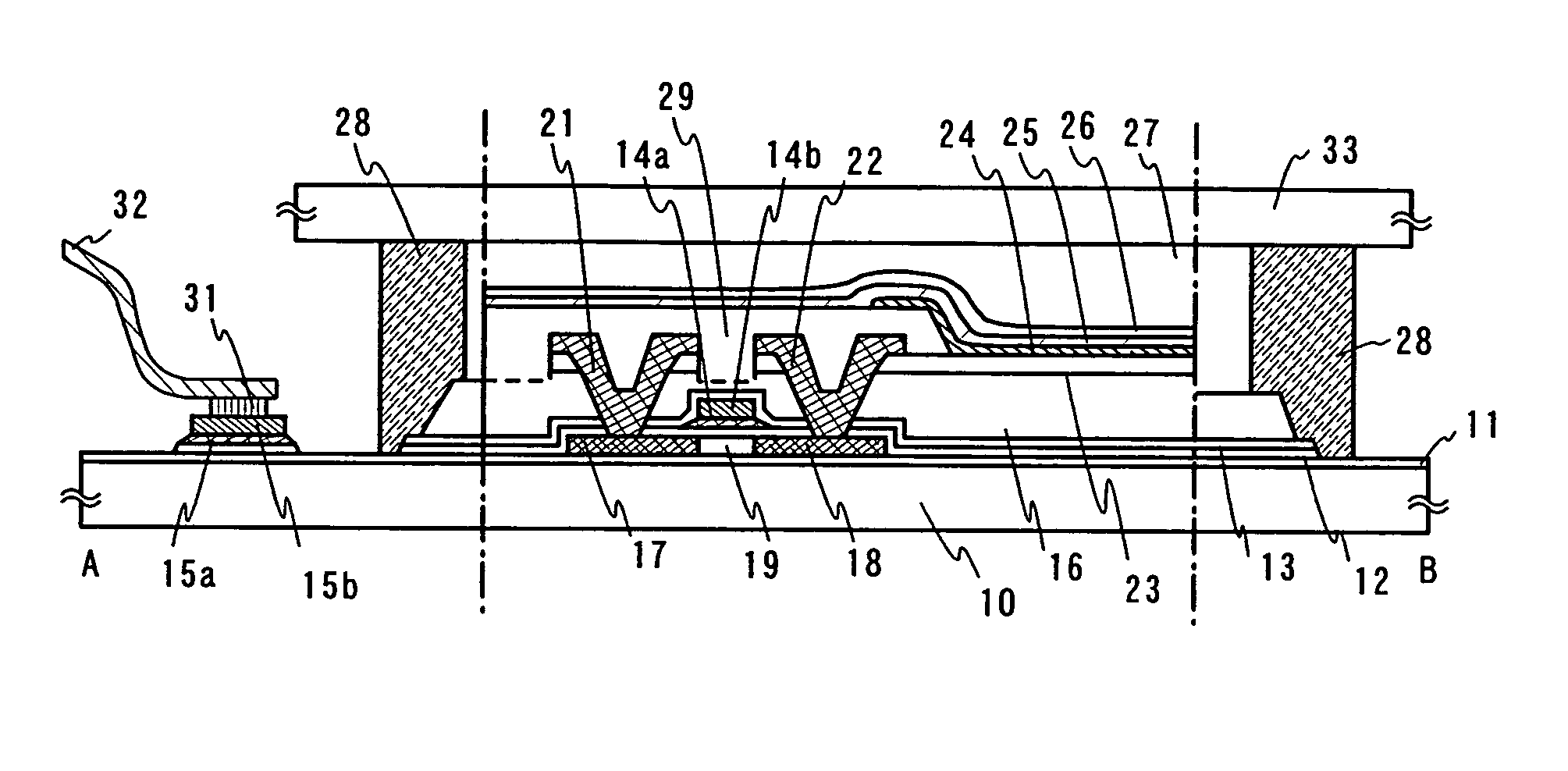
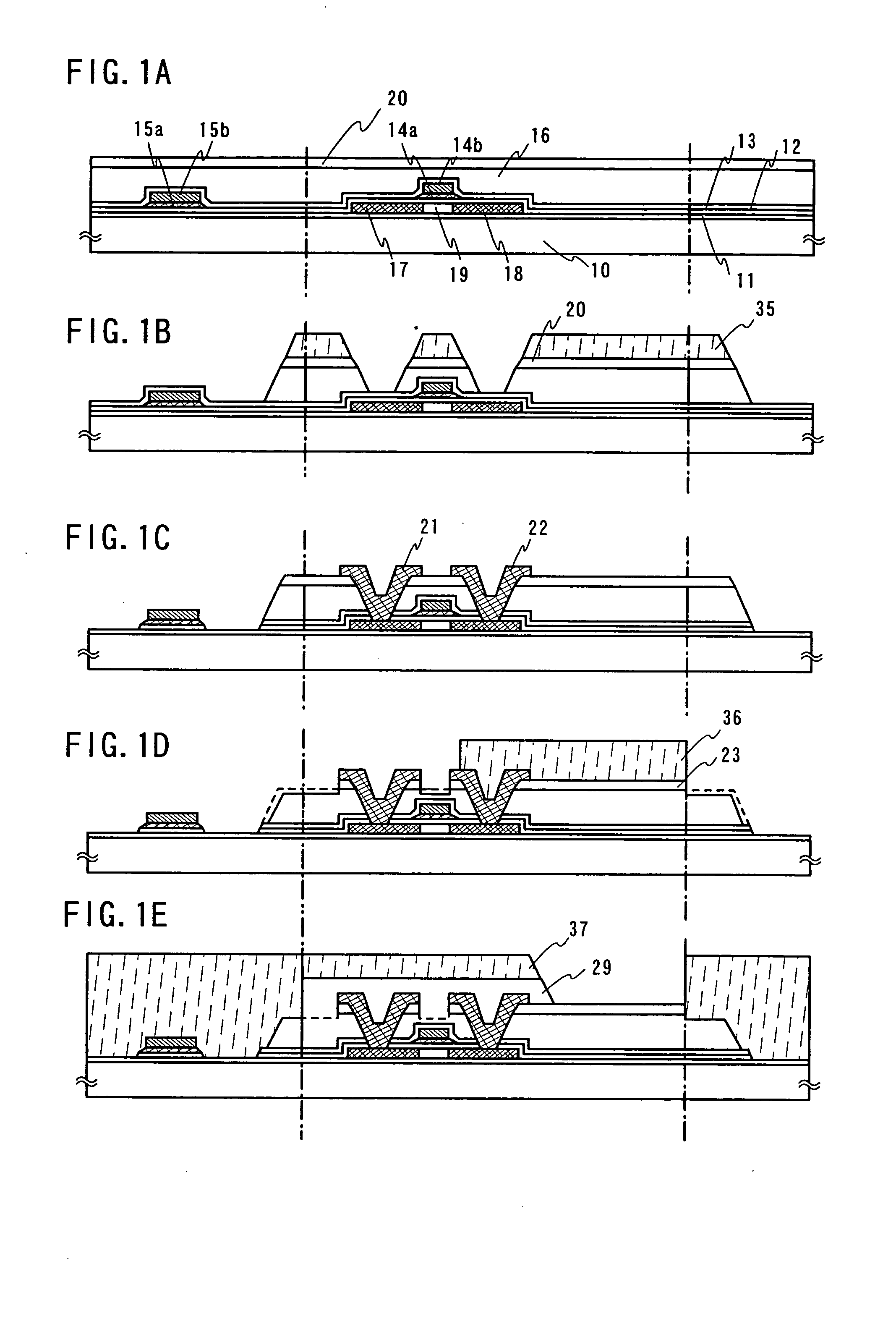
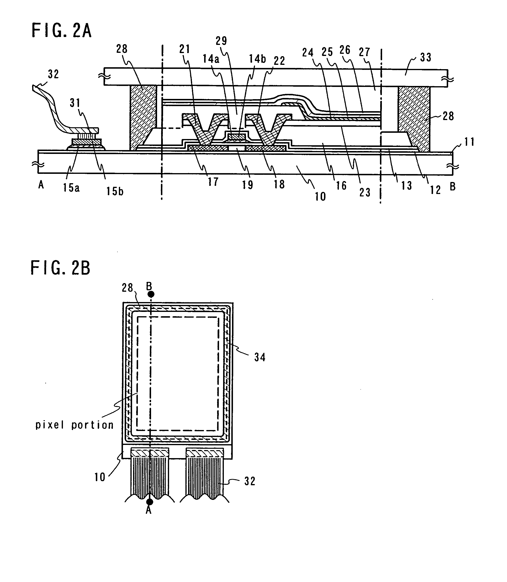
[0102] [Embodiment 1]

[0103] The present embodiment will describe an example of a bottom-emission light emitting device with reference to FIG. 4A.

[0104] A TFT connected to a light emitting element is formed on a transparent substrate (which is a glass substrate having the refractive index of about 1.55). Since the device is a bottom-emission type, interlayer insulating films, a gate insulating film, and a base insulating film are formed of materials having high light transmitting properties, respectively. As a first interlayer insulating film, a SiNO film formed by PCVD is used. As the second interlayer insulating film, a SiOx film formed by the coating method is employed.

[0105] A transparent conductive film is formed on an entire surface of the second interlayer insulating film. The transparent conductive film will serve as a first electrode 323. The transparent conductive film is formed of ITSO (100 nm in thickness), which is a transparent conductive film including SiOx. The ITSO...

embodiment 2

[0114] [Embodiment 2]

[0115] The present embodiment will describe an example of a light emitting device in which light can be emitted through both substrates with reference to FIG. 4B.

[0116] A TFT connecting to a light emitting element is formed on a transparent substrate (which is a glass substrate having the refractive index of about 1.55). In order to transmit light to display images, interlayer insulating films, a gate insulating film, and a base insulating film are formed of materials having high light transmitting properties, respectively. As for a first and third interlayer insulating films, a SiNO film formed by PCVD is used. As for a second interlayer insulating film, a SiOx film formed by the coating method is used.

[0117] A transparent conductive film is formed over an entire surface of the transparent substrate. The transparent conductive film will serves as a first electrode 423. The transparent conductive film is formed of ITSO (100 nm in thickness), which is a transpa...

embodiment 3

[0126] [Embodiment 3]

[0127] In Embodiment 3, an example of a top-emission light emitting device will be described with reference to FIGS. 6A and 6B.

[0128] An n-channel TFT connecting to a light emitting element is formed over a substrate 200 having an insulated surface. Since the top-emission light emitting device is formed in the present embodiment, interlayer insulating films, a gate insulating film 202, and a base insulating film 201 are not necessary to be formed of materials having the light emitting properties, respectively. In the embodiment, a first interlayer insulating film 210 is a SiNO film formed by PCVD, which is a highly stable material film. A second interlayer insulating film is a SiOx film formed by the coating method, which is a highly stable material film. The interlayer insulating films and the gate insulating film 202 are selectively etched to form contact holes, which reach to an active layer of the n-channel TFT. A conductive film (TiN / Al-Si / TiN) is then for...


PUM


Abstract

The present invention provides a highly stable light emitting device having high light-emitting efficiency (light-extraction efficiency) with high luminance and low power consumption, and a method of manufacturing thereof. A partition wall and a heat-resistant planarizing film are formed of a same material so as to be well-adhered to each other, thereby reducing material costs. Either an anode or a cathode is formed on the heat-resistant planarizing film. The partition wall and the heat-resistant planarizing film is adhered to each other without inserting a film having different refractive index therebetween, and therefore reflection of light is not caused in an interface.

Description

BACKGROUND OF THE INVENTION [0001] 1. Field of the Invention [0002] The present invention relates to a light emitting device having a circuit composed of a thin film transistor (hereinafter, referred to as a TFT), and a method of manufacturing thereof. For example, the invention relates to an electronic appliance mounted with a light emitting display device comprising an organic light-emitting element as a component. [0003] 2. Related Art [0004] In recent years, research related to a light emitting device having an EL element as a self-luminous light emitting element has been actively carried out. The light emitting device has also been referred to as an organic EL display or an organic light-emitting diode. Since these light emitting devices have such characteristics as rapid response speed, low voltage, low power consumption driving, which are suitable for displaying moving pictures, they have been attracting much attention for next generation displays including new-generation cel...

Claims


Application Information

Patent Timeline
IPC IPC(8): H05B33/10G09F9/30H01L21/82H01L27/15H01L27/32H01L29/22H01L29/227H01L51/50H01L51/52H01L51/56H05B33/00H05B33/12H05B33/14H05B33/22H05B33/28
CPCH01L27/3244H01L27/3246H01L51/5203H01L2251/5323H01L51/56H01L2251/5315H01L51/5262H10K59/122H10K2102/3031H10K2102/3026H10K71/00H10K59/805H10K59/131H10K59/875H10K59/12H10K50/85H10K50/805
Inventor YAMAZAKI, SHUNPEISAKAKURA, MASAYUKINAGAI, MASAHARUMATSUDA, YUTAKASAITO, KEIKOIKEDA, HISAO
Owner SEMICON ENERGY LAB CO LTD
Why Eureka
Try Eureka