Semiconductor device connecting structure, liquid crystal display unit based on the same connecting structure, and electronic apparatus using the same display unit

Inactive Publication Date: 2005-03-17
TCL CHINA STAR OPTOELECTRONICS TECH CO LTD
View PDF31 Cites 62 Cited by
  • Summary
  • Abstract
  • Description
  • Claims
  • Application Information

AI Technical Summary

Benefits of technology

[0010] According to this connecting structure, the space(s) is specially made in the bonding material when conducting the adhesion between the semiconductor device and the substrate, and absorb the deformation of the semiconductor device and others, changing freely in shape in response to the deformation of the substrate or the semiconductor device. In consequence, even in the case of the deformation of the semiconductor device or the substrate, it is possible to prevent excessive loads from applying on the electrode portions of the semiconductor device, so that the electrical connecting condition of the semiconductor device can be maintained steadily in good condition.
[0011] The space(s) is formed in the bonding material by pressurizing an IC with a pressurizing head and by heating at the same time as described below. When the temperature of the pressurizing head is given to the bonding material, the viscosity of the bonding material rapidly decreases to flow out to the external. In this way the space(s)can be formed. Thus, by forming the space(s) in the bonding material, it is possible to relieve the deformation of the semiconductor device or the substrate.
[0019] Preferably, the space rate to the adhesive assumes between 5% and 70%, more preferably between 10% and 30%. This is because, in the case that the space rate is below 5%, it is impossible to absorb the deformation (or stress) of the semiconductor device or the substrate. On the contrary, when it assumes more than 70%, the reliability of the connection between the semiconductor device and the substrate (particularly, the terminals formed on the substrate) goes down. Accordingly, if the space(s) is formed at the rate of 5% to 70%, the connection reliability can be obtained. More preferably, if the space rate is set to between 10% and 30%, the structure with improved connection reliability can be formed.
[0021] Furthermore, in accordance with the present invention, a feature of a connecting method of joining a semiconductor device onto a substrate is that a bonding layer is placed in between the substrate and the semiconductor device to join them to each other, and a pressurizing head heated up to a high temperature is pressed against the semiconductor device to pressurize and heat the mentioned bonding layer for joining the substrate to the semiconductor device, and a space(s) is formed in the mentioned bonding layer. With this construction, the deformation of the semiconductor device or the substrate can be reduced by the space(s), and a connecting structure with a higher reliability can be obtained. In addition, the bonding layer is made from an epoxy-based adhesive.
[0023] As mentioned above, it is preferable that the space rate to the adhesive is set to reach 5% to 70%, more preferably 10% to 30%, so that the semiconductor device and the electrode terminals formed on the substrate can be connected with a high reliability.

Problems solved by technology

As a result, the electrical connecting conditions can become unstable.
In addition, for avoiding such problems, the pressure-joining conditions for the liquid crystal driving IC are required to be severely managed within a small tolerance.
As a result, a complicated process management is demanded.
However, in the case of this prior connecting structure, it is required to provide the flexible bonding layer for exclusive use for the purpose of taking the cushioning action, which leads to higher component cost and manufacturing cost.

Method used


Image

  • Semiconductor device connecting structure, liquid crystal display unit based on the same connecting structure, and electronic apparatus using the same display unit
  • Semiconductor device connecting structure, liquid crystal display unit based on the same connecting structure, and electronic apparatus using the same display unit
  • Semiconductor device connecting structure, liquid crystal display unit based on the same connecting structure, and electronic apparatus using the same display unit

Examples


Embodiment Construction

[0034] The following description of the preferred embodiment(s) is merely exemplary in nature and is in no way intended to limit the invention, its application, or uses.

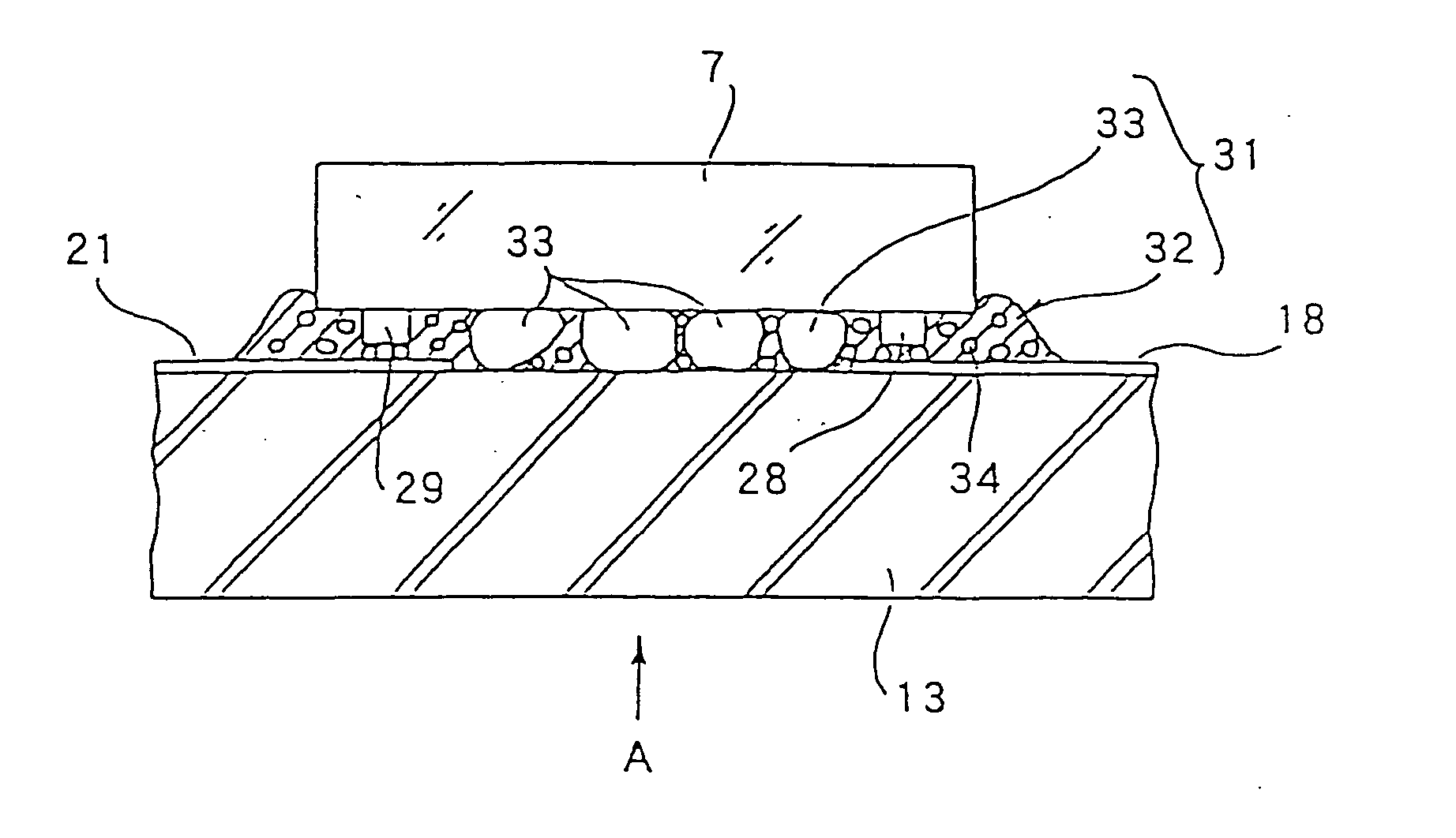
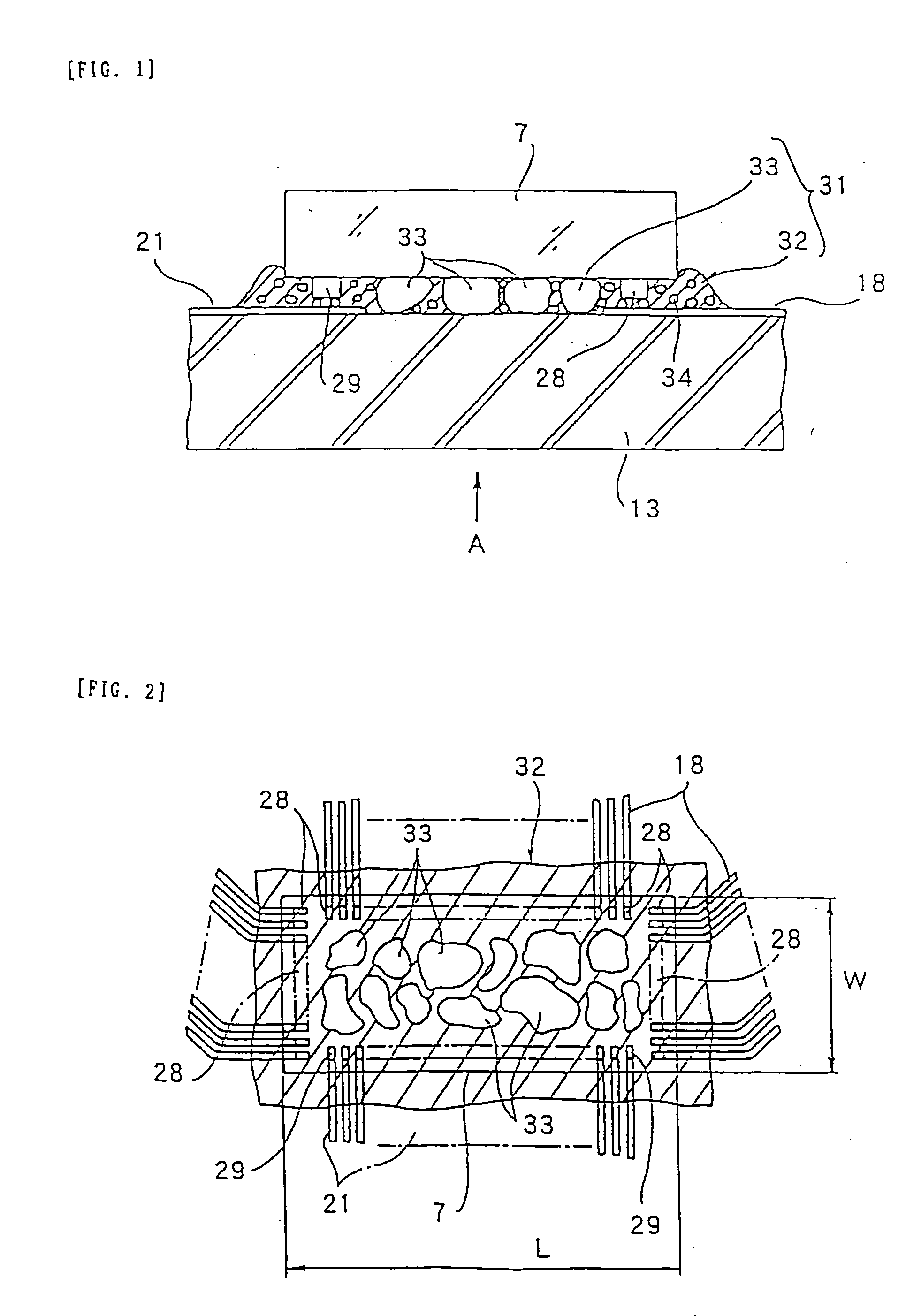
[0035]FIG. 6 shows a portable telephone as one example of electronic apparatus using a liquid crystal display unit according to an embodiment of the present invention. This portable telephone is equipped with an upper housing 1 and a lower housing 2. The upper housing 1 includes a PCB (Printed Circuit Board) for controlling a keyboard 10. In addition, the lower housing 2 includes a control circuit board 3 mounting a control LSI and a body board 4 mounting the circuit board 3. A liquid crystal display unit 5 according to this invention is mounted on the body board 4. A plurality of semiconductor driving output terminals 6 are formed as a wiring pattern on the surface of the body board 4. The liquid crystal display unit 5 has a liquid crystal driving IC 7, i.e., a semiconductor device, therein. The liquid crystal driv...


PUM


Abstract

A semiconductor device connecting structure is provided for connecting a semiconductor IC to a substrate. A bonding layer is placed between the substrate and the semiconductor IC to accomplish adhesion therebetween. Sufficient heat and pressure are applied to the bonding layer to create spaces therein which deform during relative movement between the semiconductor IC and substrate thereby maintaining consistent electrical contact between the semiconductor contact bumps and electrodes on the substrate.

Description

CROSS-REFERENCE TO RELATED APPLICATIONS [0001] This application is a divisional patent application of U.S. Ser. No. 09 / 068,270 filed May 4, 1998 which is a 371 of PCT / JP97 / 03115 filed Sep. 4, 1997 claiming priority to Japanese Application No. 8-235615 filed Sep. 5, 1996, all of which are hereby incorporated by reference.TECHNICAL FIELD [0002] The present invention relates to a semiconductor device connecting structure for connecting a semiconductor device onto a substrate (or board), a liquid crystal display unit based upon the semiconductor device connecting structure, and an electronic apparatus using the liquid crystal display unit. BACKGROUND OF THE INVENTION [0003] In recent years, liquid crystal display units for displaying visible information have come into widespread use for electronic equipment such as navigation systems, televisions, palm-top computers, electronic organizers and portable telephones. In general, these liquid crystal display units are constructed such that a...

Claims


Application Information

Patent Timeline
IPC IPC(8): G02F1/13G02F1/1343G02F1/136H01L21/52H01L21/56H01L21/60
CPCG02F1/13452H01L2924/12041H01L24/28H01L24/31H01L24/83H01L2224/16225H01L2224/73203H01L2224/8319H01L2224/838H01L2924/01004H01L2924/01015H01L2924/01027H01L2924/01033H01L2924/01049H01L2924/0105H01L2924/01074H01L2924/01078H01L2924/01082H01L2924/0781H01L2924/14H01L2924/3025H01L2224/2919H01L2924/01006H01L2924/0665H01L21/563H01L2924/00H01L2224/8385
Inventor UCHIYAMA, KENJI
Owner TCL CHINA STAR OPTOELECTRONICS TECH CO LTD
Why Eureka
Try Eureka