Fast, symmetrical XOR/XNOR gate

Inactive Publication Date: 2003-03-27
GOOGLE LLC
View PDF0 Cites 12 Cited by
  • Summary
  • Abstract
  • Description
  • Claims
  • Application Information

AI Technical Summary

Problems solved by technology

Pass gate logic circuitry in CMOS circuitry typically requires fewer transistors, resulting in smaller, faster circuits.
However, in order to avoid signal degradation, these pass gate logic circuits typically have to be enlarged because each pass gate requires two transistors instead of one, or else output buffers are needed.
Another problem with pass gate logic CMOS circuitry concerns exclusive OR ("XOR") and exclusive NOR ("XNOR") logic circuitry.
A problem with XOR and XNOR prior pass gate logic circuitry has been a lack of symmetry in structure, resulting in asymmetrical signal transitions.
This results in very non-symmetric signal transitions.
Also, it has the typical pass gate disadvantage that input signals are transmitted through pass gates to the output and thereby attenuated.
Secondly, another asymmetry arises because when both inputs are low a NFET transistor connects the output to ground, but when both inputs are high, a two transistors stack connects the output to ground.
U.S. Pat. No. 5,861,762, "Inverse Toggle XNOR and XOR Circuit," Sutherland, uses four pass gates, but is only efficient for certain applications where there exists a known order of changing input signals.

Method used


Image

  • Fast, symmetrical XOR/XNOR gate
  • Fast, symmetrical XOR/XNOR gate
  • Fast, symmetrical XOR/XNOR gate

Examples


Embodiment Construction

[0020] The claims at the end of this application set out novel features which applicants believe are characteristic of the invention. The invention, a preferred mode of use, further objectives and advantages, will best be understood by reference to the following detailed description of an illustrative embodiment read in conjunction with the accompanying drawings.

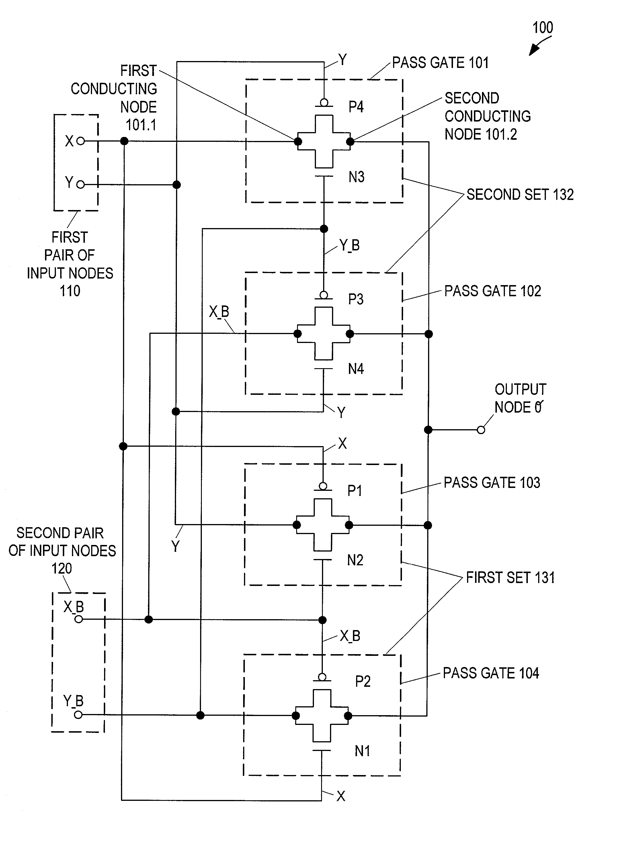
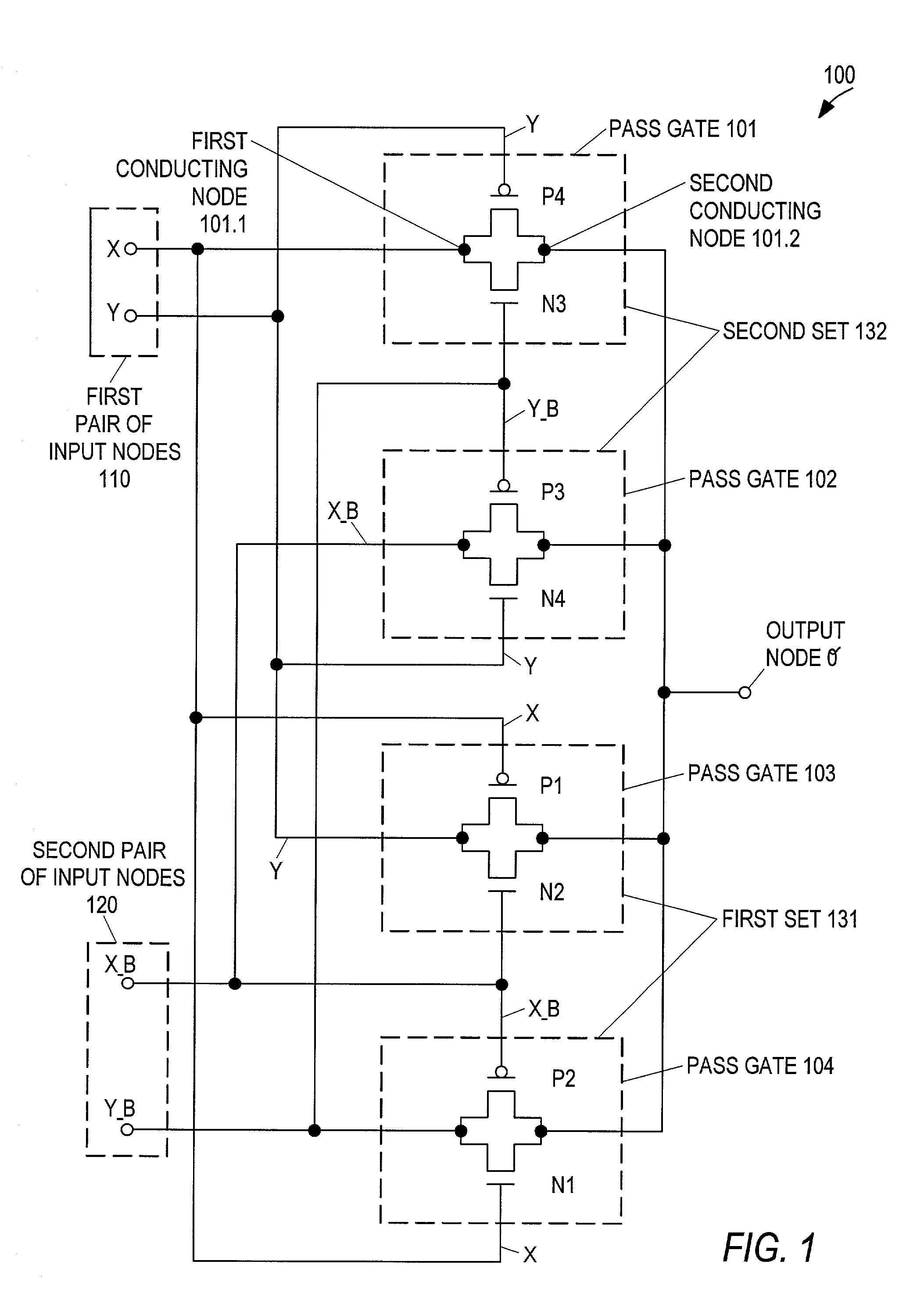
[0021] Referring now to FIG. 1 circuitry 100 is shown for an XOR or XNOR logic function, according to an embodiment. (The circuitry 100 as shown in FIG. 1 performs an XOR function as set out in the truth table 400 of FIG. 4. The complements of the inputs X and Y are not explicitly shown in the truth table 400, but they are understood. The same circuitry 100 performs the XNOR function shown in the truth table 400 if the X input is switched with its complement.) The circuitry 100 has a first pair of input nodes 110 for receiving first and second input signals, X and Y, respectively, and a second pair of input nodes 120 for rec...


PUM


Abstract

In one aspect, circuitry for a digital logic function includes a first pair of input nodes for receiving respective first and second input signals, a second pair of input nodes for receiving respective complements of the first and second input signals, and an output node. The circuitry has a plurality of PFET-NFET pass gates. Such a pass gate has a first conducting electrode of the pass gate PFET connected to a first conducting electrode of the pass gate NFET, providing a first conducting node of the pass gate, and a second conducting electrode of the pass gate PFET connected to a second conducting electrode of the pass gate NFET, providing a second conducting node of the pass gate. The input nodes are connected to first conducting nodes of respective ones of the plurality of pass gates, and the second conducting nodes of the plurality of pass gates are connected to the circuitry output node.

Description

[0001] 1. Field of the Invention[0002] This invention relates to circuitry for digital logic functions, and more particularly to pass gate circuitry for fast exclusive OR and exclusive NOR logic functions.[0003] 2. Related Art[0004] Static CMOS digital logic circuitry is very popular because it has low power consumption and it is relatively easy to design. however, it typically requires a relatively large number of transistors and the path through static CMOS logic circuitry typically includes numerous transistors in series for even a simple logic function. Pass gate logic circuitry in CMOS circuitry typically requires fewer transistors, resulting in smaller, faster circuits. However, in order to avoid signal degradation, these pass gate logic circuits typically have to be enlarged because each pass gate requires two transistors instead of one, or else output buffers are needed.[0005] Another problem with pass gate logic CMOS circuitry concerns exclusive OR ("XOR") and exclusive NOR...

Claims


Application Information

Patent Timeline
IPC IPC(8): H03K19/21
CPCH03K19/215
Inventor BOERSTLER, DAVID WILLIAMCARBALLO, JUAN ANTONIOMONTOYE, ROBERT KEVIN
Owner GOOGLE LLC
Why Eureka
Try Eureka