Chip-mounting device and method of alignment thereof

Inactive Publication Date: 2003-03-13
TORAY ENG CO LTD
View PDF4 Cites 17 Cited by
  • Summary
  • Abstract
  • Description
  • Claims
  • Application Information

AI Technical Summary

Benefits of technology

[0008] Namely, an object of the present invention is to enable a mounting speed to be increased up to a speed in a conventional mounter or a faster speed when the chip mounting device according to the present invention is applied to a bonder, thereby shortening the tact time greatly, and to enable a chip mounting accuracy to be increased up to an accuracy in a conventional bonder or a higher accuracy when the chip mounting device according to the present invention is applied to a mounter.
[0013] Further, in a case where the calibration mark is provided on a head at a position with a height different from the height of a chip held on the head, in order to remove the difficulty in focusing the second recognition means, etc. at the time of recognition and in order to shorten the time for focusing, it is preferred to adjust the height of the calibration mark to the height of chip actually held by the head at the positions of the respective recognition means. Namely, it is preferred that each head has head vertically moving means for adjusting the height of the calibration mark to the height of the chip held by the head at calibration mark reading positions of the first and second recognition means. By calibrating the position for each head, it becomes possible to store the characteristics of each head precisely.
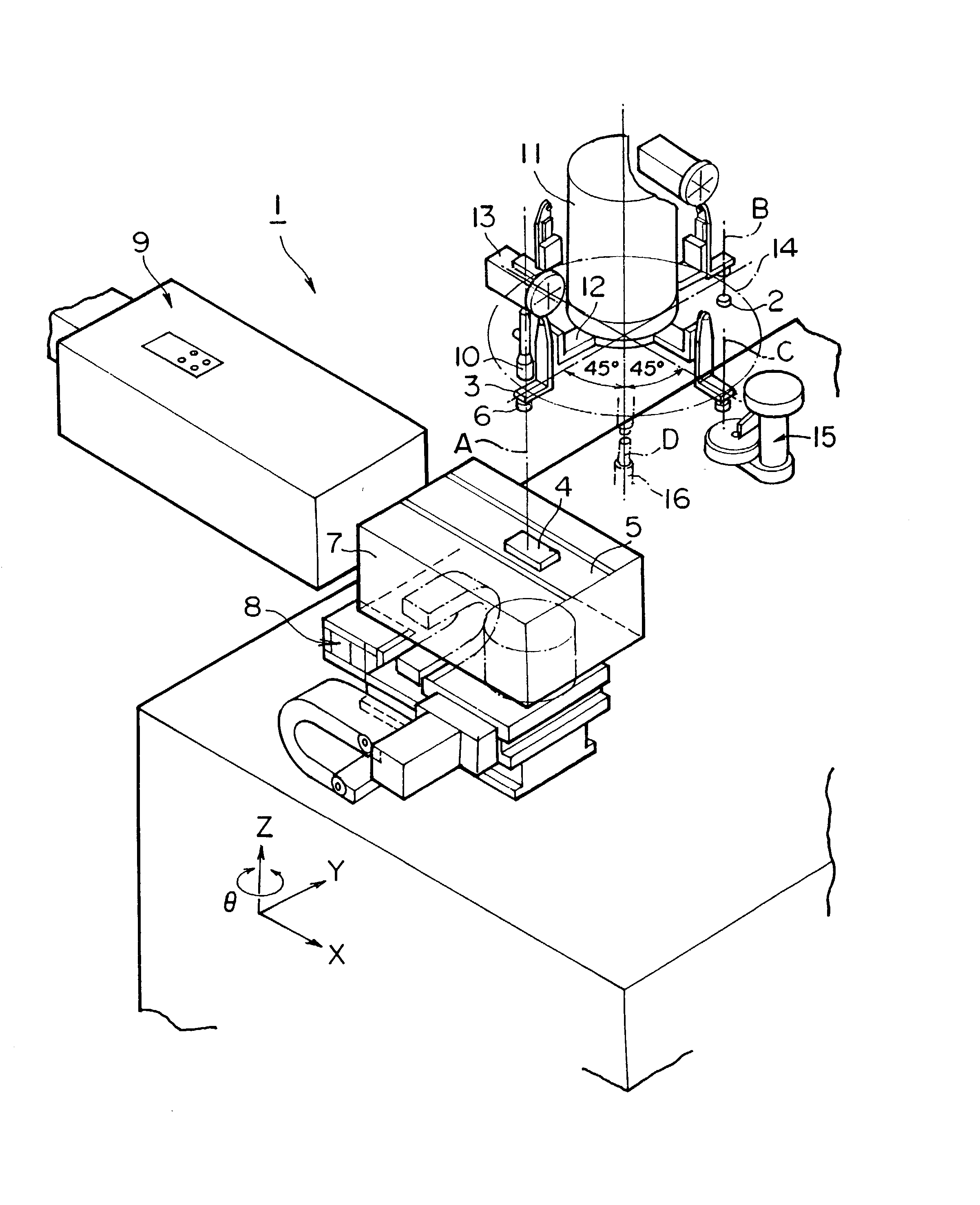
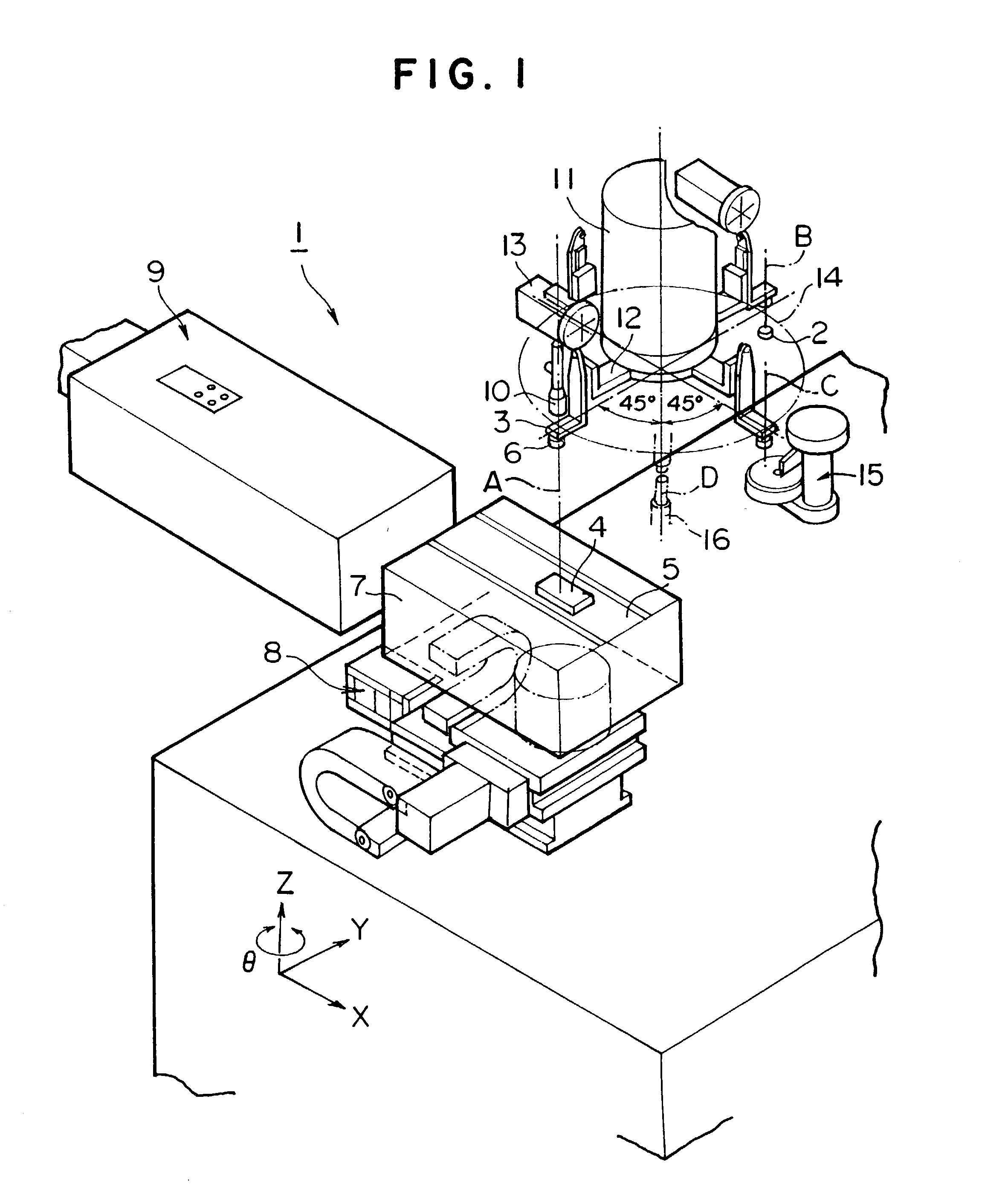
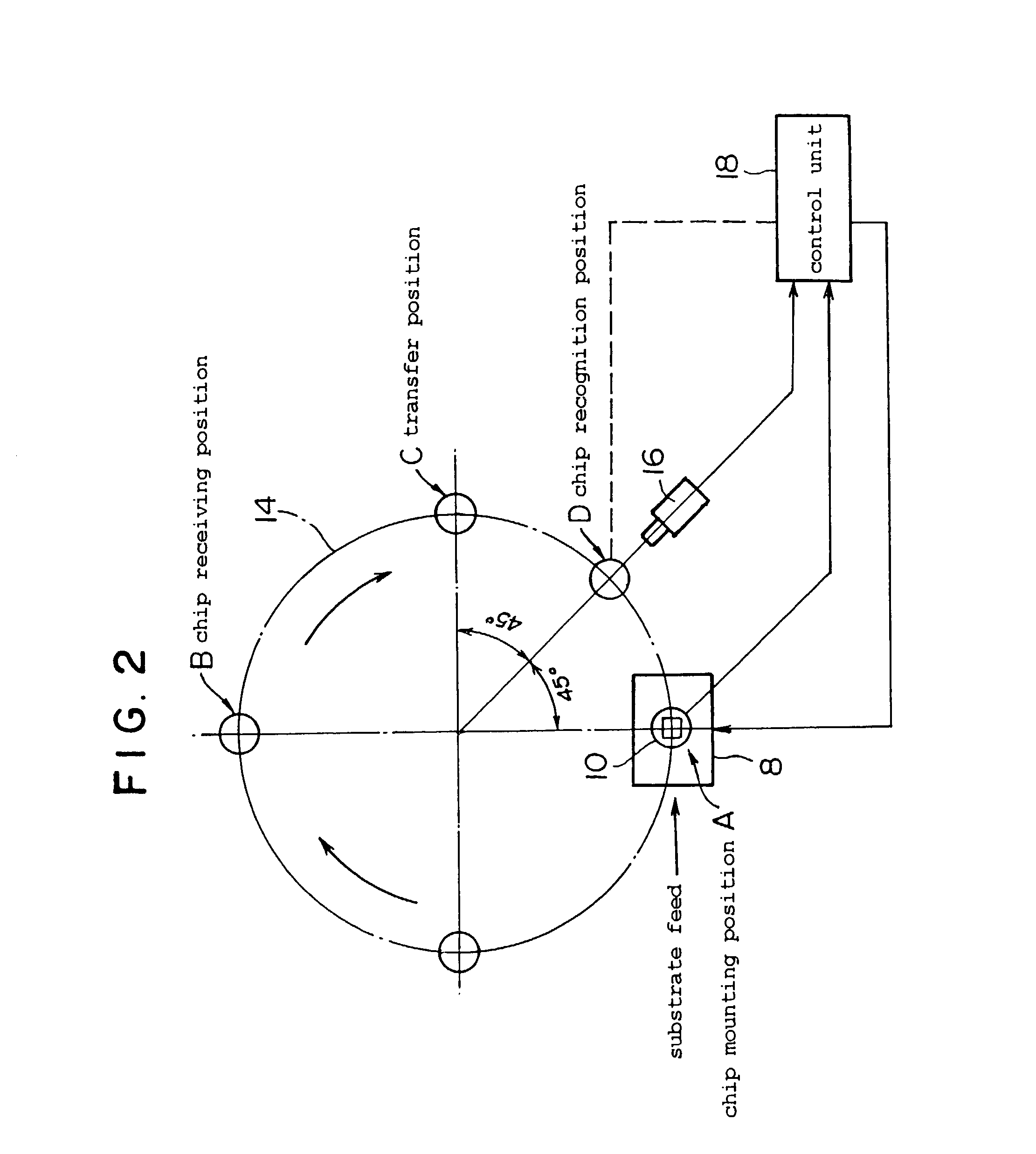
[0014] A method of alignment according to the present invention is provided as an alignment method in a chip mounting device having a plurality of heads each holding a chip, and a rotary mechanism moving the plurality of heads along a circular orbit to a plurality of positions including at least a position for receiving a chip and a position for mounting the chip onto a substrate, and the method comprises the steps of recognizing a position of the substrate on a substrate stage at a chip mounting position on the circular orbit by first recognition means; recognizing a position of the chip held on each head at a position before reaching the chip mounting position on the circular orbit, which is different from the chip mounting position, by second recognition means; and controlling the relative positional relationship between the substrate and the chip at the chip mounting position within a target accuracy.
[0017] In the above-described chip mounting device and method of alignment thereof according to the present invention, the heads are moved (rotated) from the chip receiving position to the chip mounting position onto the substrate by so-called rotary head system. In this rotary movement, the position of the chip is recognized by the second recognition means at an intermediate position before reaching the chip mounting position, and the position of the substrate is recognized by the first recognition means before the chip and the head holding the chip reach the chip mounting position. Therefore, as compared with a case of a conventional bonder wherein recognition means is inserted into and retreated from a chip mounting position and both positions of a chip and a substrate are recognized at the chip mounting position, the time of recognition of the respective positions for adjusting the relative positional relationship can be greatly shortened, the whole time of a series of operations for chip mounting can be greatly shortened, and the tact time can be shortened. Namely, it becomes possible to realize an operation speed as fast as the speed of a conventional mounter, or a faster operation speed because the substrate mark and the chip mark are read during the rotation of the rotary head.
[0018] Further, because the position of the substrate is recognized at the chip mounting position as compared with a conventional mounter, at least the accuracy in recognition of the position of the substrate may be greatly increased, and it becomes possible to realize an accuracy as high as the accuracy in a conventional bonder. In particular, if a calibration mark is provided and the same calibration mark is read at both positions of the second and first recognition means, the characteristics of heads moved toward the chip mounting position, such as the characteristic of positional shift, can be determined for each head, and therefore, an extremely high-accuracy positioning becomes possible. Namely, while the system for moving a plurality of heads successively toward the chip mounting position is employed for high-speed mounting, a precise positioning between the substrate and the chip at the chip mounting position becomes possible, and therefore, it becomes possible to realize an accuracy as high as the accuracy of a conventional bonder, or a higher accuracy.
[0019] Thus, in the chip mounting device and method of alignment thereof according to the present invention, a high-speed mounting at an operation speed in a conventional mounter or a faster operation speed becomes possible, and at the same time, a high-accuracy mounting at an accuracy in a conventional bonder or a higher accuracy becomes possible. Therefore, particularly, the tact time of a bonder can be greatly shortened, and the chip mounting accuracy of a mounter can be greatly increased.

Problems solved by technology

On the contrary, because the two-sight recognition means is inserted and retreated at a chip mounting position, other operations cannot be performed during its operation, whereby there is a limit in shortening of the time of a series of operations in the device.
Therefore, even if the device is constructed as a rotary-head type chip mounting device as described above, there is a limit in shortening of the tact time.
However, because an amount in shift of the relative position is not amended at the actual chip mounting position, the bonding accuracy between the substrate and the chip is not improved so much, and the accuracy is limited to about 100 .mu.m at highest.
Although such a mounter has been used for applications that do not require a high accuracy, recently the demand for high accuracy in a mounter has been increased, and therefore, the conventional mounter cannot satisfy the requirement.

Method used


Image

  • Chip-mounting device and method of alignment thereof
  • Chip-mounting device and method of alignment thereof
  • Chip-mounting device and method of alignment thereof

Examples


Embodiment Construction

[0025] Hereinafter, desirable embodiments of the present invention will be explained referring to figures.

[0026] FIGS. 1 to 3 show a chip mounting device according to an embodiment of the present invention. In FIG. 1, chip mounting device 1 has a plurality of heads 3 each holding a chip 2 by suction, etc., and a substrate holding stage 5 (substrate stage) provided below the head for holding a substrate 4 such as a circuit board or a liquid crystal panel by suction, etc. Head 3 holds chip 2 by attraction, etc. on the lower surface of a tool 6 provided at the lower end of the head 3. When chip mounting device 1 is constructed as a bonder, tool 6 is structured so as to be able to heat by being incorporated with a heater, and when it is constructed as a mounter, a heater is not incorporated. Namely, tool 6 may be structured in a form either with a heater or without a heater.

[0027] In this embodiment, substrate holding stage 5 is fixed on a slide table 7, and a chip mounting position on ...


PUM

PropertyMeasurementUnit
Heightaaaaaaaaaa

Abstract

A mounting device (1) including a plurality of heads (3), each holding a chip (2), arranged on a circle, is used to realize accurate and high-speed mounting. A mounting device comprises a plurality of heads (3) with calibration marks, first recognition means (10) fixed in a chip mounting position (A), and second recognition means (16) fixed in another position. Prior to mounting operation, the first recognition mechanism and the second recognition mechanism recognize and store the positions of the calibration marks of the heads (3) In mounting operation, the first recognition means (10) recognizes the positions of a substrate (4) and the calibration marks of the heads (3), whereas the second recognition means (16) recognizes the positions of chips (2) attracted on the heads (3). The heads are moved vertically to adjust plane to be recognized. The chip (2) and the substrate (4) are aligned according to the position information obtained by the recognition mechanisms, and the chips are mounted.

Description

[0001] The present invention relates to a chip mounting device and a method of alignment thereof, and specifically to a chip mounting device capable of performing high-speed and accurate alignment and an alignment method in the chip mounting device.BACKGROUND ART OF THE INVENTION[0002] As well known, in a conventional chip mounting device, the position of a chip held by a head and the position of a substrate (for example, a liquid crystal panel, etc.) supported by a substrate holding stage disposed below the head are precisely positioned, and in this condition, chip mounting is performed by moving the head down.[0003] In order to raise the working efficiency of the mounting operation and shorten the tact time in such a chip mounting device, is known a so-called rotary-head type chip mounting device wherein a plurality of heads are provided and each head is moved in order between a position for receiving a chip and a position for mounting the chip onto a substrate (for example, JP-A-...

Claims


Application Information

Patent Timeline
IPC IPC(8): H01L21/52H05K13/04H05K13/08
CPCH05K13/0413H05K13/08Y10T29/53087Y10T29/49131Y10T29/4913Y10T29/53174Y10T29/53178H05K13/089H05K13/041H01L21/60
Inventor TERADA, KATSUMIYAMAUCHI, AKIRA
Owner TORAY ENG CO LTD
Why Eureka
Try Eureka