
Oled current drive pixel circuit

a technology of organic light-emitting diodes and current-driven pixel circuits, which is applied in the direction of static indicating devices, instruments, solid-state devices, etc., can solve the problems of non-zero operating voltage of amorphous silicon for a substantially larger volume, and the inability to drive oleds with nfet-configured current sources

Inactive Publication Date: 2002-12-26
INNOLUX CORP
View PDF3 Cites 380 Cited by
  • Summary
  • Abstract
  • Description
  • Claims
  • Application Information

AI Technical Summary

Problems solved by technology

Large area crystalline silicon back planes would not be as cost effective as amorphous or polysilicon.
Due to a manner in which OLEDs are processed, it is not normally possible to drive OLEDs with an NFET configured current source.
However, for driving OLEDs requiring continuous current for operation, the amorphous silicon operating voltages are non-zero for a substantially larger percentage of the time, e.g., duty cycles of up to 100%.
The higher voltages and continuous current severely stresses the amorphous silicon TFT.
In particular, a gate to source voltage stress causes a threshold voltage to vary due to trapped charging and other effects such as creation of defect states and molecular bond breakage at a gate insulator-to-semiconductor interface and in a semiconductor layer of the TFT.
A higher level of 5% luminance variation is typically considered to be unacceptable.
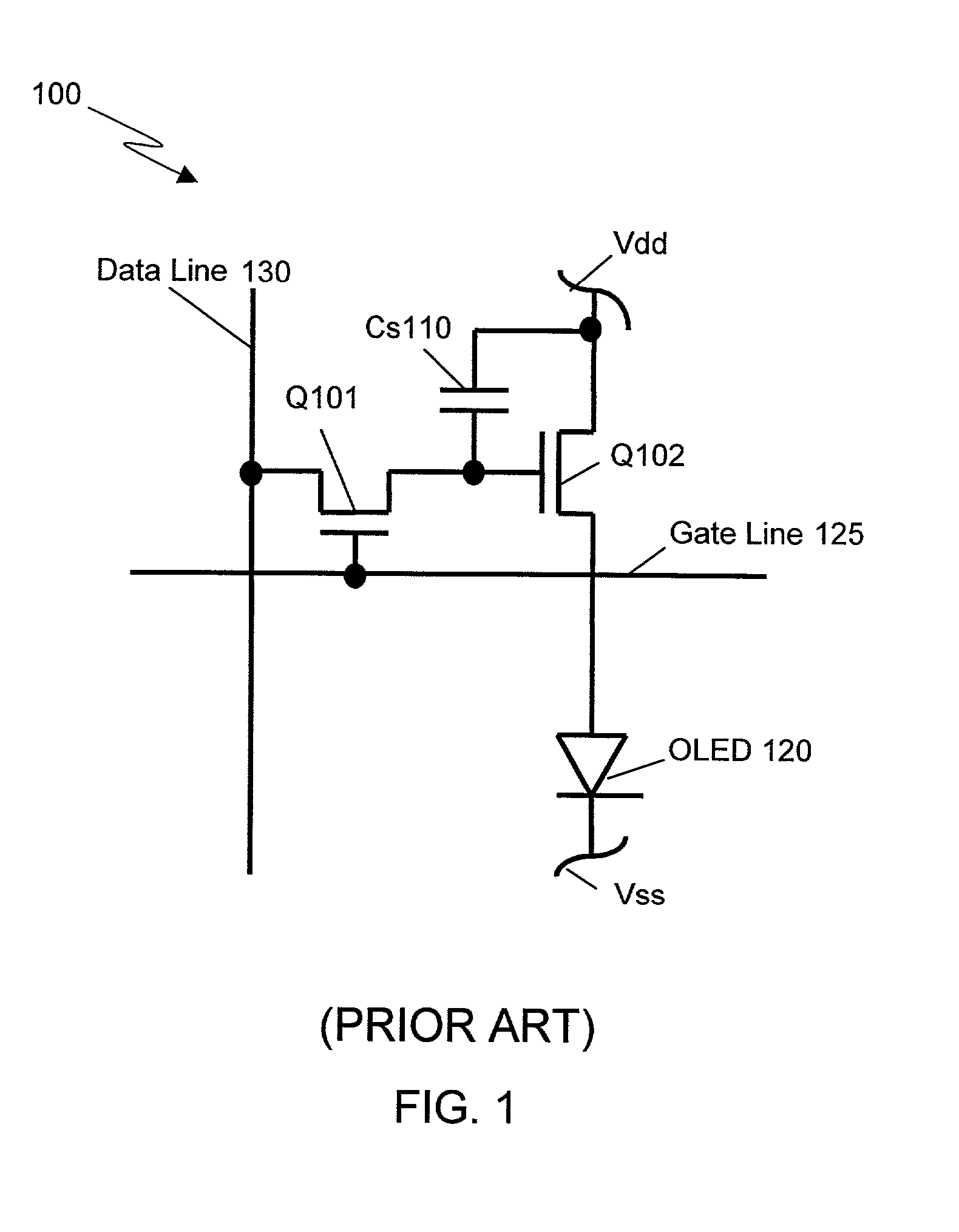
The threshold variation of NFET Q102, which requires continuous current for operation, is considered unacceptable for many applications.
However, the Sony circuit does not correct for threshold variation of an OLED driving transistor.
The elimination of the third input does not allow its use in high-resolution displays having dark gray scale capability.
One limitation of this circuit is that a second transistor is connected in series with an OLED current generating transistor to a power supply.

Method used


Image

  • Oled current drive pixel circuit
  • Oled current drive pixel circuit
  • Oled current drive pixel circuit

Examples


Embodiment Construction

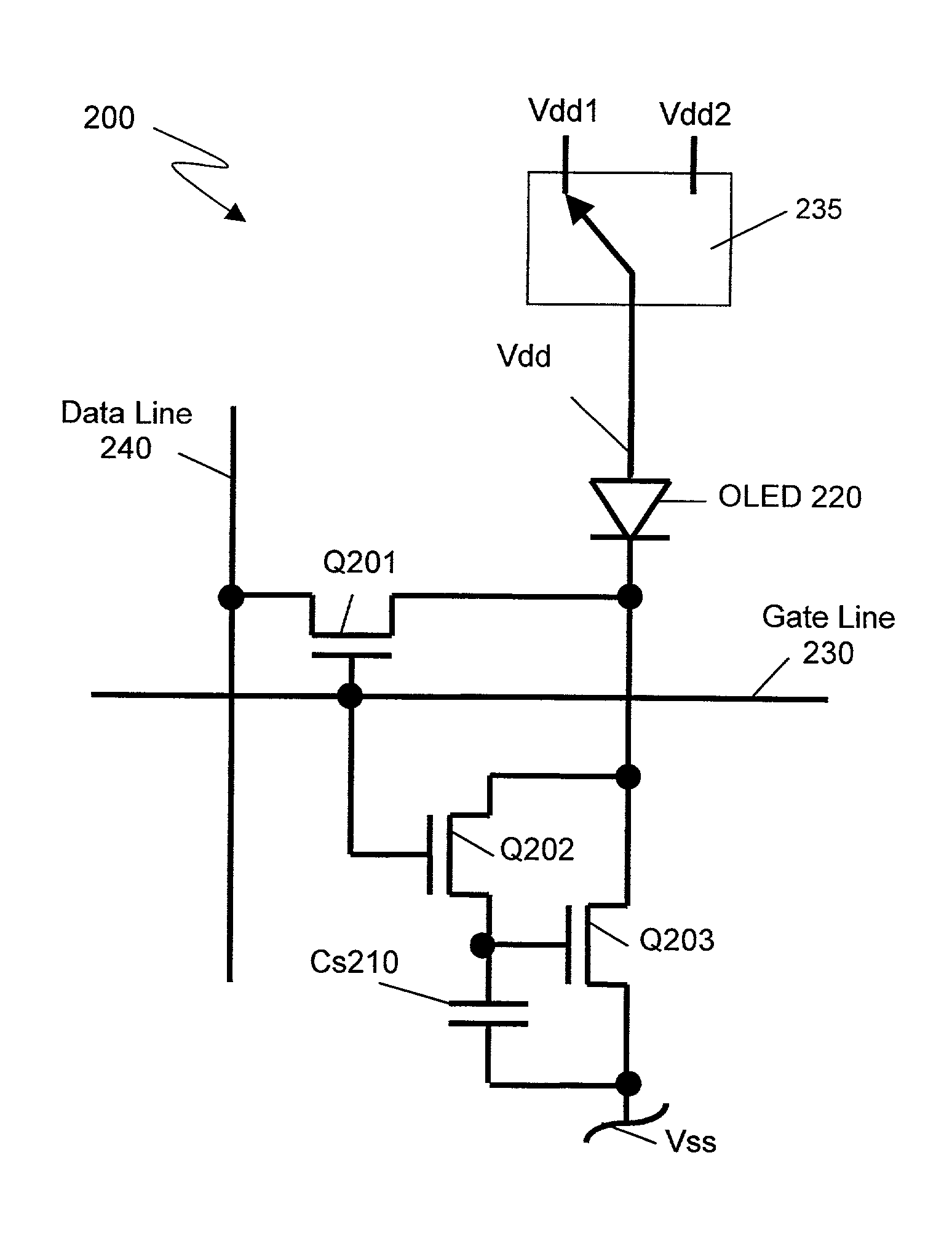
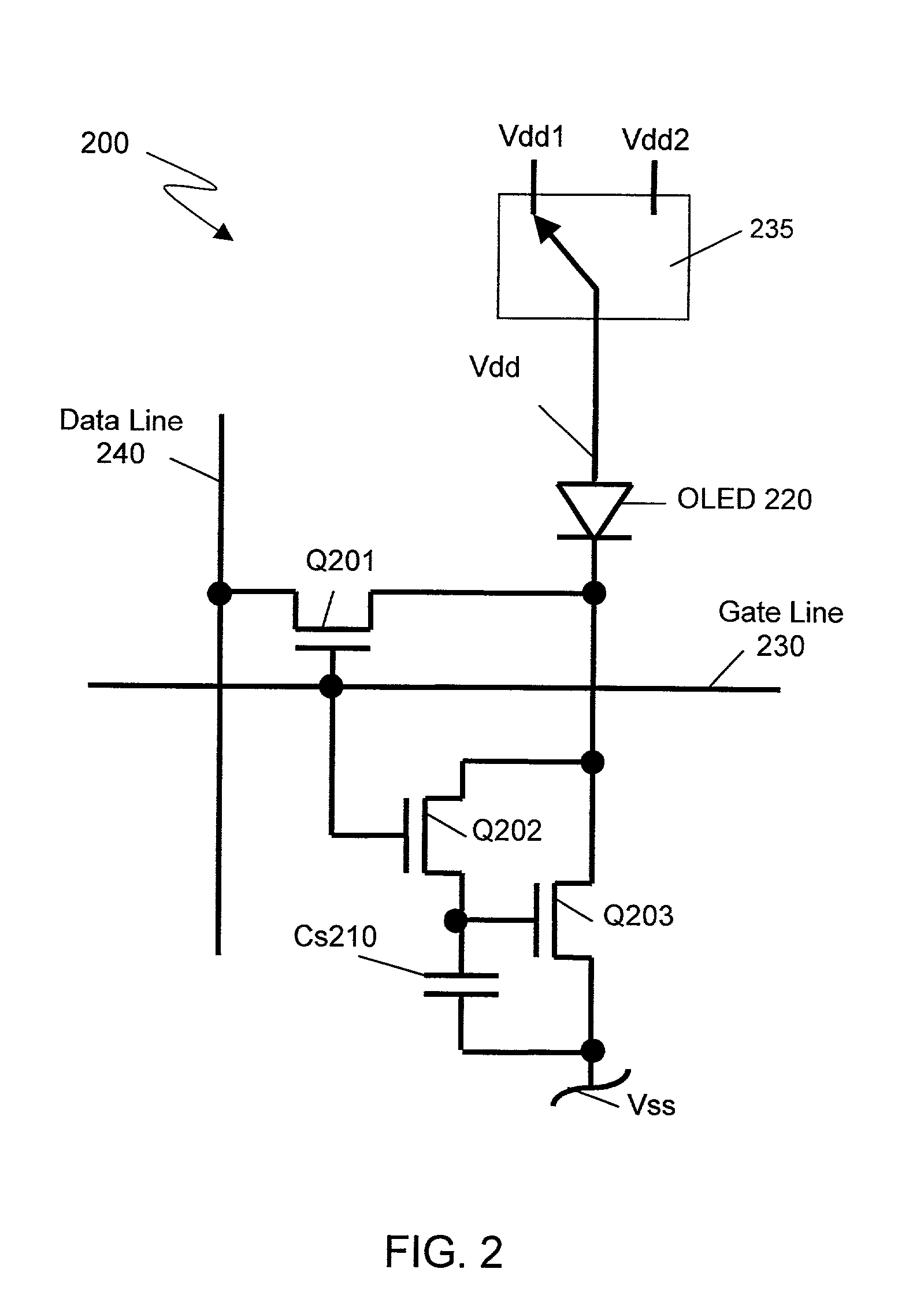
[0030] The present invention provides for a technique of driving a pixel circuit that minimizes stress effects of a TFT device that provides current to an OLED. Current driving is used to write a voltage stored in the pixel circuit. The circuit corrects for threshold variation of the TFT device. OLED current passes through a single transistor while allowing dark gray scale capability with high-resolution displays.

[0031] FIG. 2 is a schematic of a pixel circuit 200 being driven in accordance with the present invention. Using data line current, a current through an OLED can accurately be established with a 3 NFET circuit that can accommodate threshold voltage or mobility variations. Circuit 200 includes NFETS Q201, Q202 and Q203, a data storage capacitor Cs210, an OLED 220 and a switch 235. Circuit 200 also includes a gate line 230, a data line 240, and supply voltages Vdd and Vss.

[0032] Switch 235 operates to apply or direct a first signal (Vdd1) to an anode terminal of OLED 220 when...


PUM


Abstract

There is provided a method for driving an organic light emitting diode (OLED) pixel circuit. The method includes applying a first signal to a terminal of the OLED when setting a state of the pixel circuit, and applying a second signal to the terminal when viewing the state. There is also provided a driver for an OLED pixel circuit, where the driver employs this method.

Description

[0001] The present application is claiming priority of U.S. Provisional Patent Application Ser. No. 60 / 300,216, filed on Jun. 22, 2001.[0002] 1. Field of the Invention[0003] The present invention relates to an organic light emitting diode (OLED) pixel circuit, and more particularly, to a technique for driving the pixel circuit that minimizes stress effects of a TFT device that provides current to the OLED.[0004] 2. Description of the Prior Art[0005] An organic light emitting diode (OLED) pixel may utilize any of a variety of organic materials that emit light when an electric current is applied thereto. An OLED display comprises a plurality of OLED pixels organized into an array.[0006] One method to achieve a large size and large foro at OLED display is to use an active matrix thin film transistor (TFT) back plane. A head mount display and even a direct view display for a small mobile application may use polysilicon or crystalline silicon as a back plane. Due to investments in amorph...

Claims


Application Information

Patent Timeline
Patent Type & Authority Applications(United States)
IPC IPC(8): H01L51/50G09G3/20G09G3/30G09G3/32
CPCG09G3/3233G09G3/325G09G2300/0842G09G2320/043G09G2310/0256G09G2320/02G09G2300/0866G09G3/30
Inventor SANFORD, JAMES LAWRENCELIBSCH, FRANK ROBERT
Owner INNOLUX CORP
Learn More