Coupled-cap flip chip BGA package with improved cap design for reduced interfacial stresses
a flip chip and interfacial stress technology, applied in the field of electronic packages, can solve the problems of not maintaining package flatness, indicating a bit poor thermal conductivity, and a modulus lower than that of steel
- Summary
- Abstract
- Description
- Claims
- Application Information
AI Technical Summary
Benefits of technology
Problems solved by technology
Method used
Image
Examples
Embodiment Construction
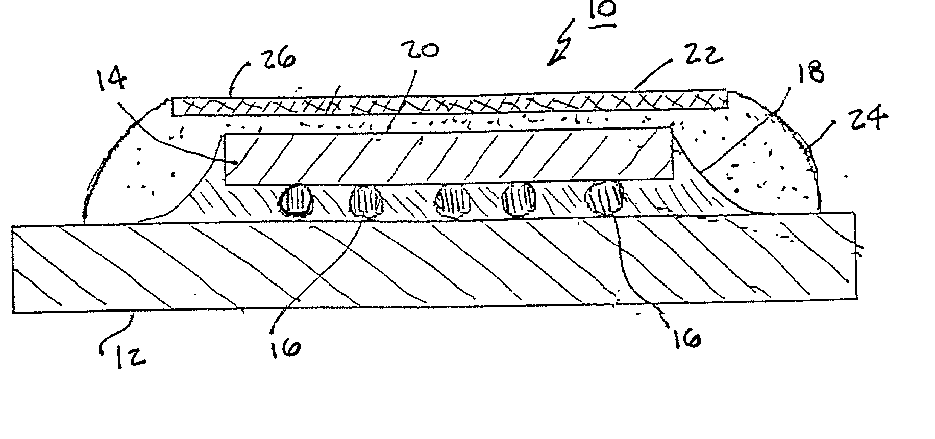
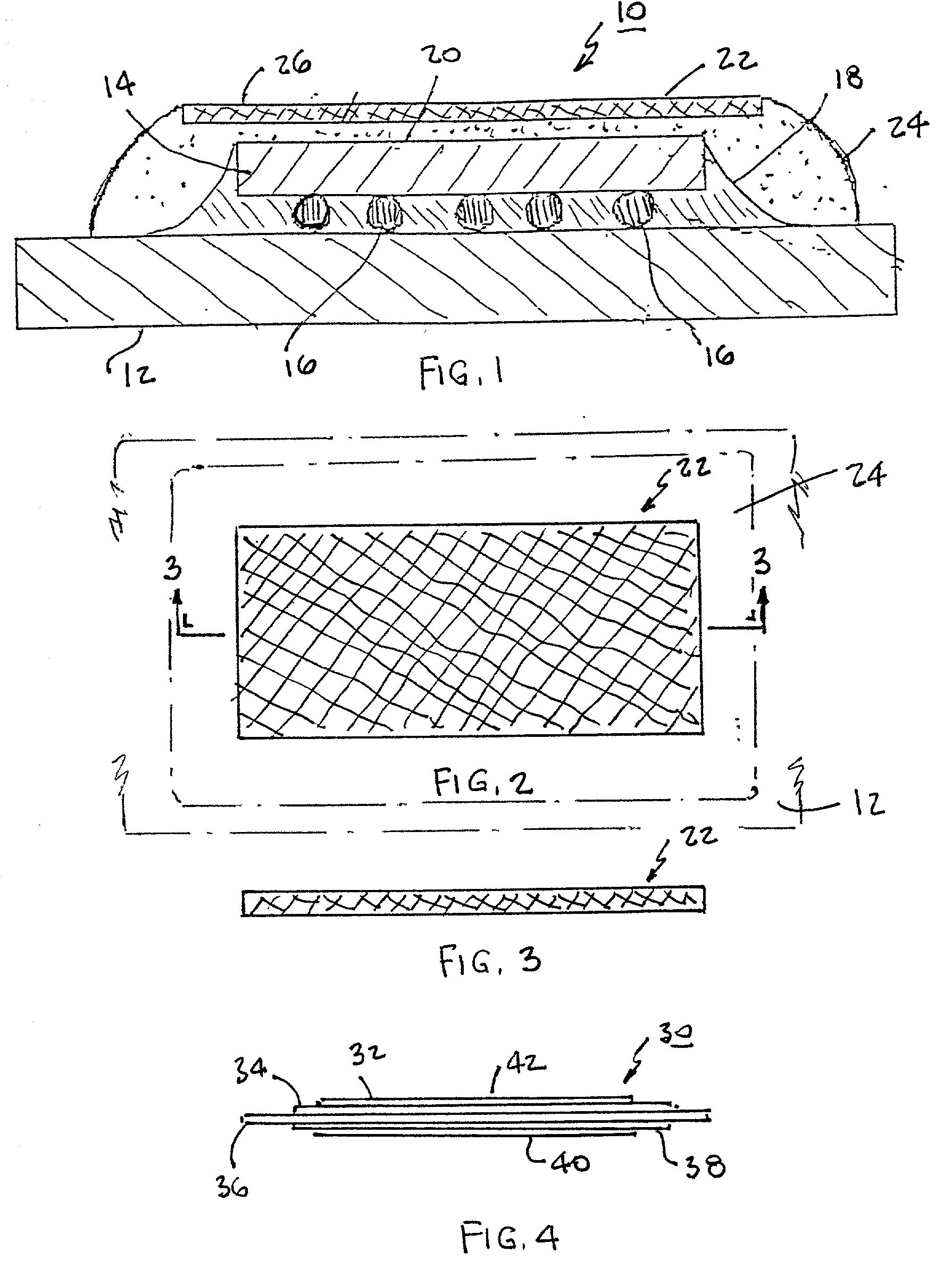
[0027] Reverting in detail to the drawings, and particularly to FIG. 1, there is disclosed an electronic package comprising a semiconductor chip package or module 10 which essentially includes a circuitized substrate 12, which may be constituted of an organic material or laminate. Positioned above the circuitized substrate 12 is a semiconductor chip 14, which is electrically coupled to the substrate 12, for example through the intermediary of solder ball controlled collapse chip connections (C4) 16, and with the provision of an underfill 18 between components 12 and 14, as shown in the drawing.
[0028] In turn, positioned above the semiconductor chip 14 so as to face the surface 20 of the latter in closely spaced relationship is a cover or cap structure 22, which in this instance is shown as being constituted of a flat or planar member, preferably of rectangular or square configuration in plan view relative to the peripheral configuration of the semiconductor chip 14.
[0029] As illustr...
PUM
 Abstract
Description
Claims
Application Information
 - R&D Engineer
- R&D Manager
- IP Professional
- Industry Leading Data Capabilities
- Powerful AI technology
- Patent DNA Extraction
Browse by: Latest US Patents, China's latest patents, Technical Efficacy Thesaurus, Application Domain, Technology Topic, Popular Technical Reports.
© 2024 PatSnap. All rights reserved.Legal|Privacy policy|Modern Slavery Act Transparency Statement|Sitemap|About US| Contact US: help@patsnap.com


