
Power semiconductor module

a technology of semiconductor modules and semiconductor devices, applied in semiconductor devices, semiconductor/solid-state device details, electrical apparatus, etc., can solve problems such as the risk of cracking solder

Active Publication Date: 2022-11-15
HITACHI ENERGY SWITZERLAND AG
View PDF25 Cites 0 Cited by
  • Summary
  • Abstract
  • Description
  • Claims
  • Application Information

AI Technical Summary

Benefits of technology

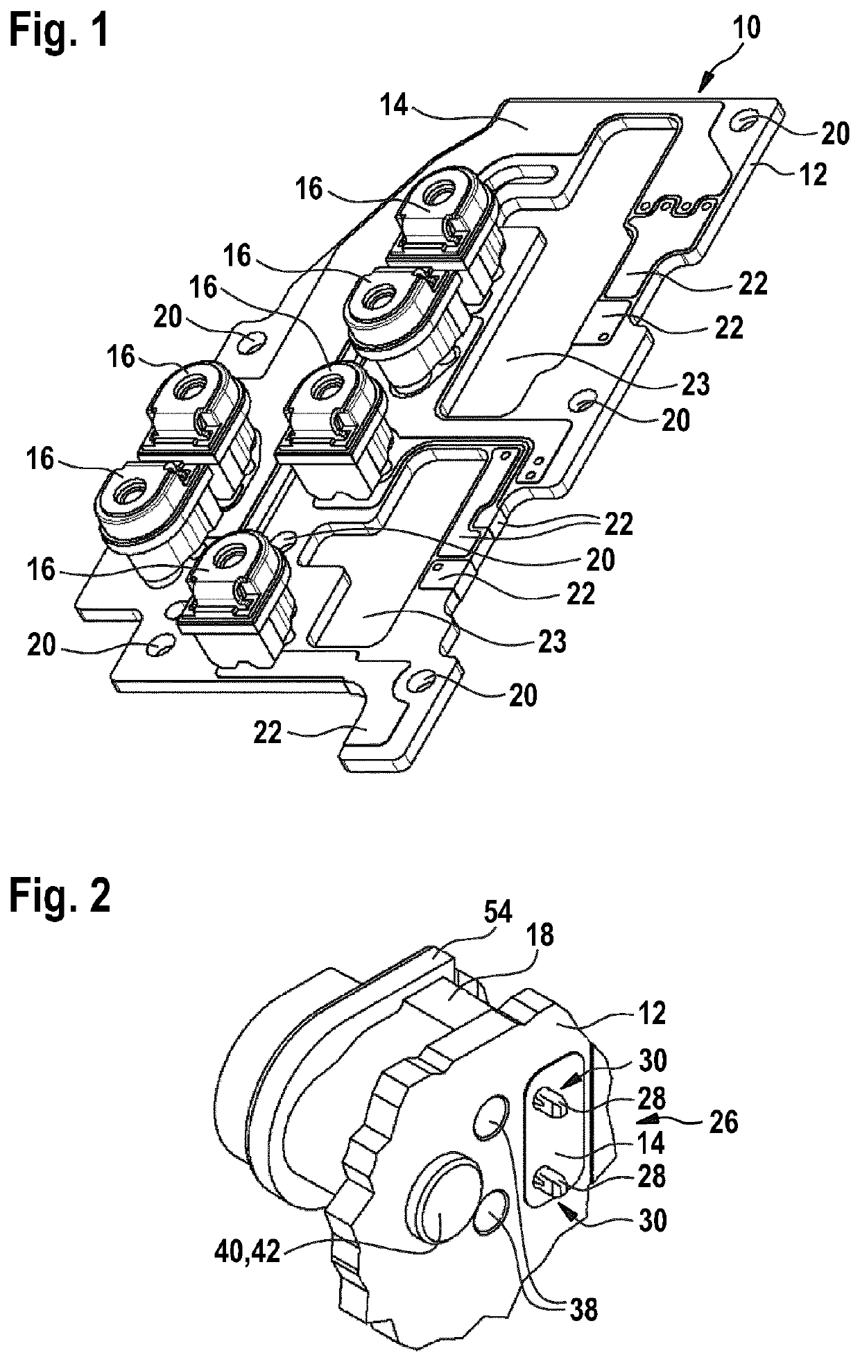
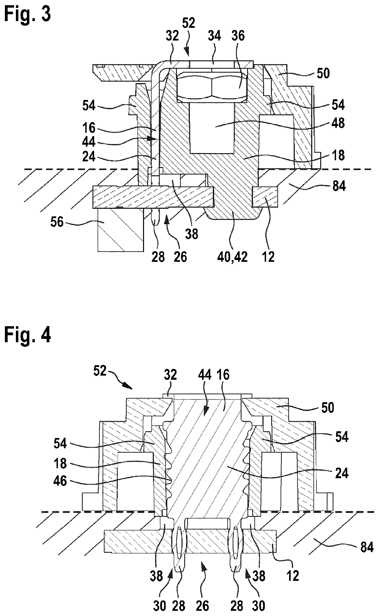
The objective of the patent is to create a reliable, flexible and cost-effective power semiconductor module that has auxiliary terminals bent over nuts.

Problems solved by technology

However, there may be still a risk of creating cracks in the solder due to high stress.

Method used


Image

  • Power semiconductor module
  • Power semiconductor module
  • Power semiconductor module

Examples


Embodiment Construction

[0011]It is an objective of the invention to provide a reliable, flexible and economic power semiconductor module, which has auxiliary terminals bent over nuts.

[0012]This objective is achieved by the subject-matter of the independent claims. Further exemplary embodiments are evident from the dependent claims and the following description.

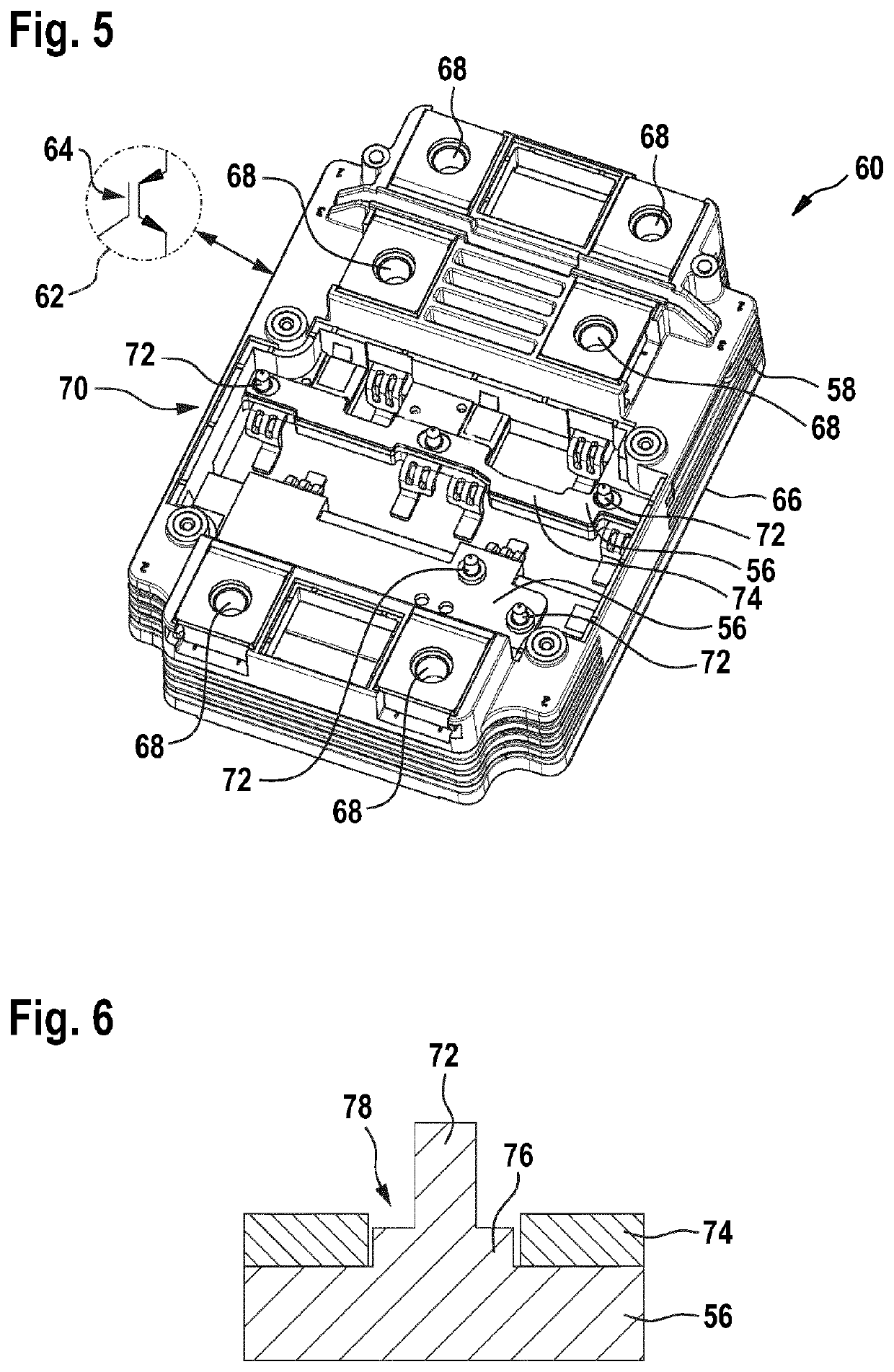
[0013]The invention relates to a power semiconductor module. A semiconductor module may be any device composed of one or more semiconductor chips, their electrical and mechanical interconnections and a housing for these components. The term “power” here and in the following may refer to modules and / or semiconductor chips adapted for processing current of more than 100 V and / or more than 10 A.

[0014]According to an embodiment of the invention, the power semiconductor module comprises a housing accommodating a power circuit with at least one power semiconductor chip, which housing provides at least two power terminals. For example, the housing may be m...


PUM

PropertyMeasurementUnit
currentaaaaaaaaaa
thicknessaaaaaaaaaa
thicknessaaaaaaaaaa

Abstract

A power semiconductor module includes a housing accommodating a power circuit with at least one power semiconductor chip, the housing providing at least two power terminals; a printed circuit board mounted to the housing and electrically connected to the power circuit for distributing auxiliary signals; and at least one auxiliary terminal mounted to the printed circuit board with a press-fit connection provided by a body of the auxiliary terminal.

Description

FIELD OF THE INVENTION[0001]The invention relates to a power semiconductor module.BACKGROUND OF THE INVENTION[0002]A power semiconductor module accommodates one or more power semiconductor chips, which may be electrically connected with terminals provided on a housing of the power semiconductor module. Power terminals are used for interconnecting conductors carrying the load current of the power semiconductor module. Auxiliary terminals, which usually have a much lower current rating as the power terminals, are used for supplying gate signals, accessing sensor signals, etc.[0003]Some power semiconductor modules have a printed circuit board on which the auxiliary terminals are provided. The printed circuit board is electrically connected to the interior of the power semiconductor module and the auxiliary terminals may be soldered to the printed circuit board. The auxiliary terminals may protrude through a module cover above the printed circuit board and the auxiliary terminals may be...

Claims


Application Information

Patent Timeline
Patent Type & Authority Patents(United States)
IPC IPC(8): H01R12/58H05K3/30H01L23/498
CPCH01R12/585H01L23/49811H05K7/14329
Inventor TRUESSEL, DOMINIKHARTMANN, SAMUELFISCHER, FABIANBEYER, HARALD
Owner HITACHI ENERGY SWITZERLAND AG
Learn More