Display panel with separated pixel circuit regions

a technology of pixel circuit regions and display panels, applied in the field of display panels, can solve the problems of affecting the display effect, grating effect occurs easily in such designs, drawbacks exist in conventional technologies,

Active Publication Date: 2022-09-13
SHENZHEN CHINA STAR OPTOELECTRONICS SEMICON DISPLAY TECH CO LTD
View PDF7 Cites 0 Cited by
  • Summary
  • Abstract
  • Description
  • Claims
  • Application Information

AI Technical Summary

Benefits of technology

[0004]The present disclosure provides a display panel which can reduce grating effect of the display panel in order to enhance transparent display effect of the display panel.
[0032]The beneficial effects are as following. The display panel of the present disclosure separates the pixel circuit regions from each other by adjusting the arrangement of the pixel circuit regions (non-transparent regions) of the pixels; thereby, the pixel circuit regions are prevented from being arranged in an entire row. As a result, grating effect of the display panel is weakened and the transparency of the display panel is improved. On the other hand, the area of transparent regions is maximized by adopting the arrangement of the present disclosure. In the meanwhile, the transparency of the display panel is improved.

Problems solved by technology

However, grating effect occurs easily in such designs when the display panel is lit.
As a result, it seems that there are dense dark lines in images, thereby affecting the display effect.
Therefore, drawbacks exist in the conventional technologies, and improvements are urgently required.

Method used


Image

  • Display panel with separated pixel circuit regions
  • Display panel with separated pixel circuit regions

Examples


Embodiment Construction

[0037]The following description of the various embodiments is provided with reference of drawings to illustrate specific embodiments. Directional terms mentioned in the present disclosure, such as upper, lower, front, back, left, right, inside, outside, lateral, etc., are only referring to the direction of the drawing. Therefore, the directional terms used to describe and clarify the present disclosure should not be viewed as limitations of the present disclosure. In the drawing, structurally similar elements are denoted by the same reference numbers.

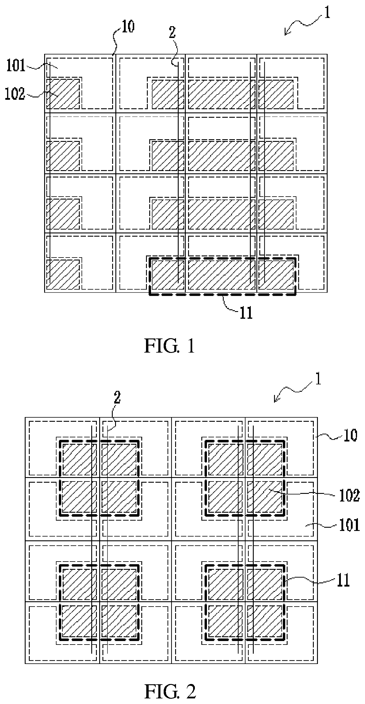
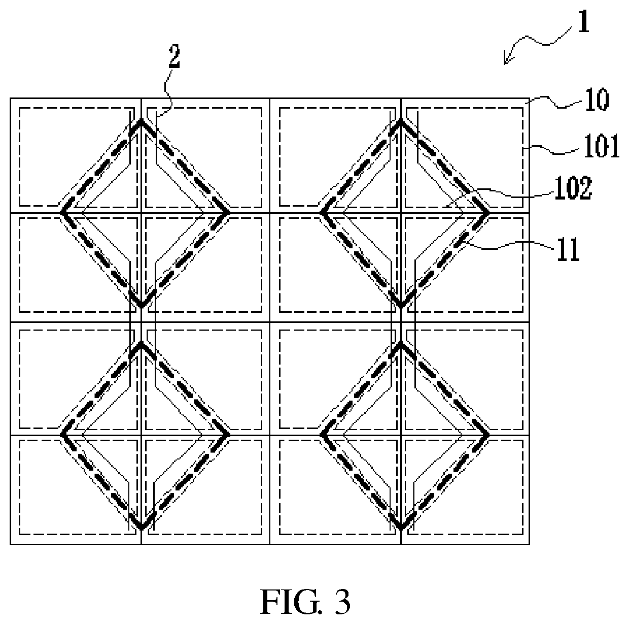
[0038]The present disclosure focuses on grating effect occurring in the existing display panels, which results from the bar-shape designs of the pixel circuit regions and transparent regions. The grating makes images have dense dark lines, thereby affecting the display effect. The present disclosure can solve these drawbacks.

[0039]The display panel of the present disclosure is a transparent display panel. The display panel includes a ba...


PUM


Abstract

The present disclosure provides a display panel including gate lines and data lines disposed on a base substrate. The base substrate is further divided into pixel regions including transparent regions and pixel circuit regions having pixel circuits. The pixel circuit regions of at least two adjacent pixel regions are disposed next to each other and form a pixel circuit joining region, so that the pixel circuit regions of a same row or a same column of the pixel regions are arranged spaced apart from each other. Two adjacent pixel circuit joining regions are spaced apart by the transparent regions.

Description

FIELD OF INVENTION[0001]The present disclosure relates to the field of display technology, more particularly, to a display panel.BACKGROUND OF INVENTION[0002]In conventional transparent display panel designs, a single pixel region includes a transparent region and a non-transparent region. The transparent region is transparent for light transmission. The non-transparent region includes a pixel circuit region. In conventional designs, the pixel circuit regions and the transparent regions are often in shapes of strips. However, grating effect occurs easily in such designs when the display panel is lit. As a result, it seems that there are dense dark lines in images, thereby affecting the display effect.[0003]Therefore, drawbacks exist in the conventional technologies, and improvements are urgently required.SUMMARY OF INVENTION[0004]The present disclosure provides a display panel which can reduce grating effect of the display panel in order to enhance transparent display effect of the ...

Claims


Application Information

Patent Timeline
Patent Type & Authority Patents(United States)
IPC IPC(8): H01L27/32
CPCH01L27/326H10K59/121H10K59/131
Inventor XIAO, XIANGHAN, BAIXIANG
Owner SHENZHEN CHINA STAR OPTOELECTRONICS SEMICON DISPLAY TECH CO LTD
Why Eureka
Try Eureka