Electronic device including guide member for facilitating assembling or separation of electronic component

a technology of electronic components and guide members, which is applied in the field of electronic devices, can solve the problems of reducing the utilization efficiency of inner space of electronic devices and damage to electronic components, and achieve the effect of facilitating assembling (or separating) of electronic components and reducing the amount of spa

Active Publication Date: 2022-05-03
SAMSUNG ELECTRONICS CO LTD
View PDF39 Cites 0 Cited by
  • Summary
  • Abstract
  • Description
  • Claims
  • Application Information

AI Technical Summary

Benefits of technology

[0006]The avoidance space may mean ‘a space for allowing the lens barrel to move without interference with another structure in an operation of assembling or separating an electronic component (e.g., a camera module)’. As the number of electronic components mounted on the electronic device becomes larger, the number of the avoidance spaces becomes larger. However, because the avoidance space substantially cannot be utilized after the electronic components are assembled, the inner space utilization efficiency of the electronic device may be lowered. When a plurality of electronic components is disposed while being exposed through the avoidance spaces, the electronic components may be damaged due to physical contacts in the assembling or separation process, and electromagnetic interference may be caused in the operations of the electronic components. In some embodiments, the avoidance space increases the thickness of the structure (e.g., the internal structure of the housing) of the electronic device and has a form of a through-hole, lowering the strength of the electronic device.
[0007]Various embodiments of the disclosure may provide an electronic device which facilitates assembling or separation of an electronic component while preventing interference with an internal structure during assembling of the electronic component and has an improved strength by reducing an avoidance space.
[0034]The electronic device according to various embodiments of the disclosure can prevent interference with an electronic component (e.g., a camera module) and an internal structure while not forming a separate avoidance space and facilitate assembling (or separation) of an electronic component by guiding the electronic component by using a guide member when the electronic component is mounted.
[0035]According to various embodiments of the disclosure, because the internal structures of the electronic device can spatially and electrically isolate the electronic components as the avoidance space is reduced, a physical contact or an electromagnetic interference between the electronic components can be alleviated and prevented in the assembling or separation process.

Problems solved by technology

However, because the avoidance space substantially cannot be utilized after the electronic components are assembled, the inner space utilization efficiency of the electronic device may be lowered.
When a plurality of electronic components is disposed while being exposed through the avoidance spaces, the electronic components may be damaged due to physical contacts in the assembling or separation process, and electromagnetic interference may be caused in the operations of the electronic components.

Method used


Image

  • Electronic device including guide member for facilitating assembling or separation of electronic component
  • Electronic device including guide member for facilitating assembling or separation of electronic component
  • Electronic device including guide member for facilitating assembling or separation of electronic component

Examples


Embodiment Construction

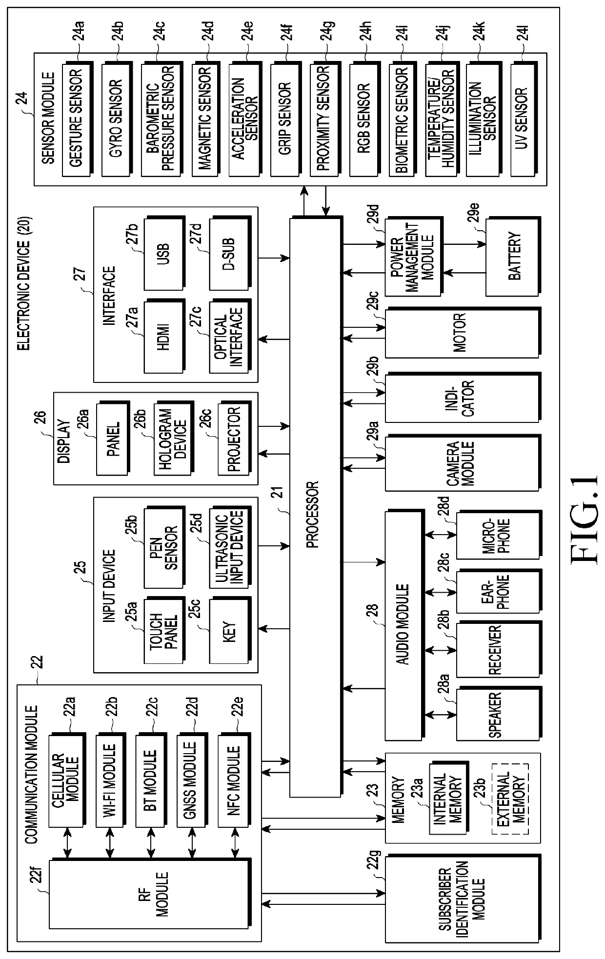
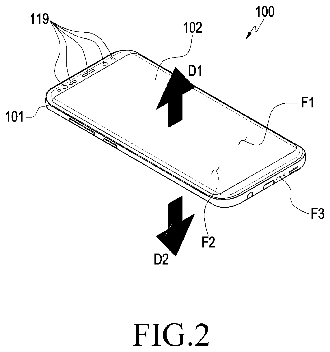
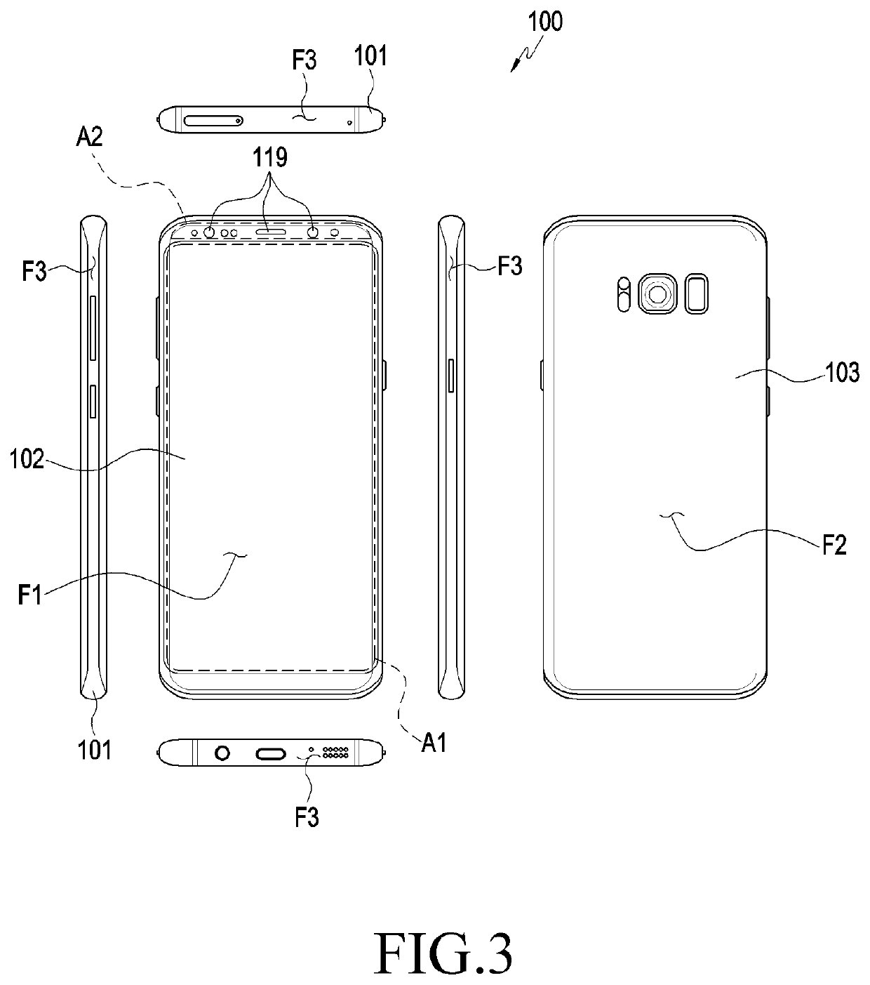
[0060]As the disclosure allows for various changes and numerous embodiments, some exemplary embodiments will be described in detail with reference to the accompanying drawings. However, the disclosure is not limited to specific disclosed forms, but it is understood that the scope of the disclosure include all changes pertaining to the spirit and technical scope of the disclosure, equivalents or replacements thereof.

[0061]The terms including ordinal numbers, such as ‘first’ and ‘second’, may be used to describe various elements, but the elements are not limited to the terms. The terms may be used only for the purpose of distinguishing one element from another element. For example, without departing the scope of the disclosure, a first element may be referred to as a second element, and similarly, a second element may be referred to as a first element. The term of ‘and / or’ includes a combination of a plurality of related items described or any one of a plurality of related items descr...


PUM


Abstract

According to various embodiments of the present invention, an electronic device may comprise: a housing which comprises a first surface facing in a first direction, a second surface facing in a second direction opposite to the first direction, and a side wall at least partially surrounding a space between the first surface and the second surface; at least one seating part formed to be partially surrounded by a part of the side wall inside the housing; a guide member disposed adjacent to a part of the side wall inside the housing and surrounding another part of the seating part; and at least one electronic component comprising a body part and a protrusion part formed on one surface of the body part, wherein the electronic component may be guided by the guide member to enter the seating part along a direction inclined with respect to the side wall or the first surface and then to be mounted in the seating part. The electronic device as described above may vary depending on embodiments.

Description

CROSS-REFERENCE TO RELATED APPLICATIONS[0001]This application is a U.S. National Stage application under 35 U.S.C. § 371 of an International application filed on Dec. 27, 2017 and assigned application number PCT / KR2017 / 015541, which claimed the priority of a Korean patent application filed on Mar. 15, 2017 in the Korean intellectual Property Office and assigned Serial number 10-2017-0032638, the entire disclosure of which is hereby incorporated by reference.BACKGROUND1. Field[0002]The disclosure relates to an electronic device, and for example, relates to an electronic device including an electronic component.2. Description of Related Art[0003]Electronic components capable of coping with various functions while being small-sized and lightweight for securing portability have been mounted on electronic devices. For example, while electronic components such as microphones, speaker phones, camera modules, and display devices for inputting and outputting sounds, videos, and images have b...

Claims


Application Information

Patent Timeline
Patent Type & Authority Patents(United States)
IPC IPC(8): H04M1/02H05K9/00H04N5/225G06F3/041
CPCH04M1/0249H04M1/0264H04M1/0266H04N5/2254H05K9/0081G06F3/0412G06F1/1658G06F1/1626H04M2250/12H04M1/026H04N23/00H04M2250/02H04M2250/06H04M2201/38H04N23/55
Inventor HA, SEON-WOOLEE, SANG-KYULEE, JUNG-HOONSUNG, TAE-HYUNYOON, BYOUNG-UK
Owner SAMSUNG ELECTRONICS CO LTD
Why Eureka
Try Eureka