
Transparent conductive film, manufacturing method of a transparent conductive film and touch panel

a manufacturing method and technology of transparent conductive film, applied in the direction of instruments, electric digital data processing, input/output process of data processing, etc., can solve the problems of signal loss and distortion, poor flexibility of thin-film metal meshes, and easy breakage, etc., to achieve good transmittance, improve bending characteristics, and reduce the effect of sheet resistan

Active Publication Date: 2022-04-05
CAMBRIOS FILM SOLUTIONS CORP
View PDF8 Cites 0 Cited by
  • Summary
  • Abstract
  • Description
  • Claims
  • Application Information

AI Technical Summary

Benefits of technology

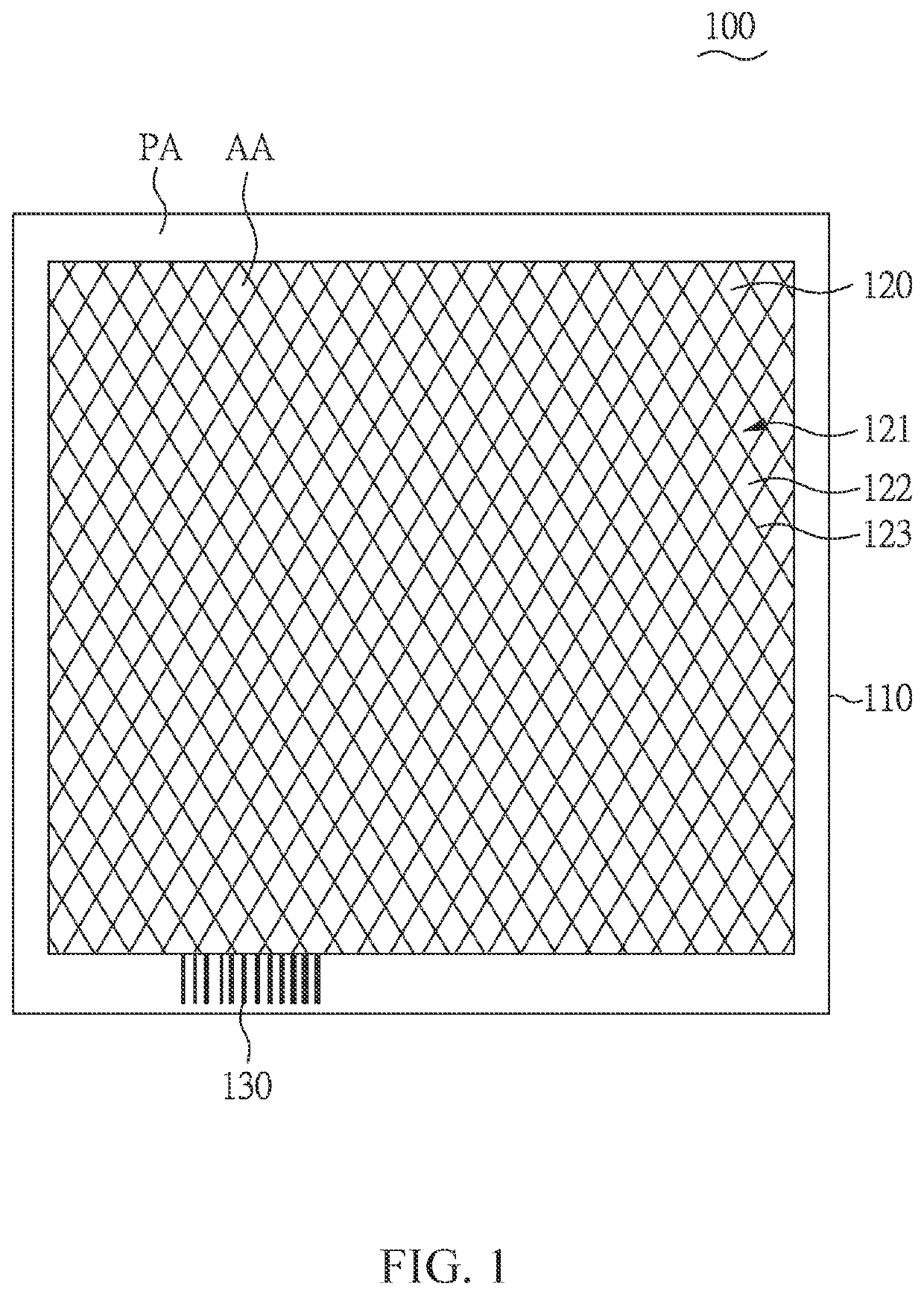
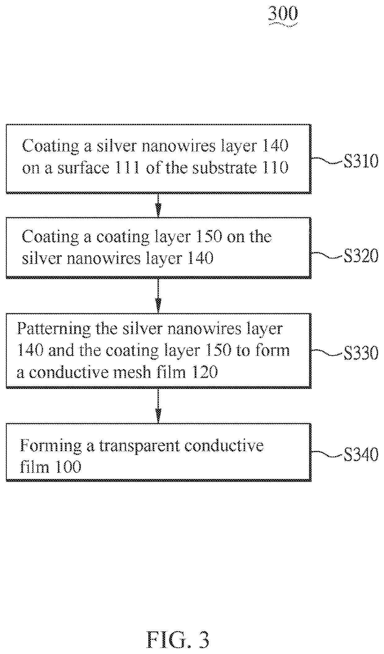
The present patent discloses a new transparent conductive laminated structure and touch panel that use silver nanowires mesh film. This film has ultra-low sheet resistance and good transparency. It also has better bending characteristics. By using this mesh film, the problem of contact impedance between metal wires and silicon nanowires is solved, reducing signal loss and distortion. The manufacturing process is simplified, and the cost is lower. The touch panel is environmentally friendly. In summary, this patent introduces a new technology that simplifies the production of flexible and transparent touch panels.

Problems solved by technology

However, the metal mesh made of thin-film metal has poor flexibility and is easily broken due to bending.
Moreover, in general, the metal mesh made of thin-film metal requires additional metal wires to connect with the lines in the peripheral area, and the combination of the metal mesh and the additional metal wires will generate higher resistance, causing signal loss and distortion.

Method used


Image

  • Transparent conductive film, manufacturing method of a transparent conductive film and touch panel
  • Transparent conductive film, manufacturing method of a transparent conductive film and touch panel
  • Transparent conductive film, manufacturing method of a transparent conductive film and touch panel

Examples


Embodiment Construction

[0029]The following disclosure provides many different embodiments, or examples, for implementing different features of the disclosure. Specific examples of components and arrangements are described below to simplify the present disclosure. These are, of course, merely examples and are not intended to be limiting. In addition, the present disclosure may repeat reference numerals and / or letters in the various examples. This repetition is for the purpose of simplicity and clarity and does not in itself dictate a relationship between the various embodiments and / or configurations discussed.

[0030]It will be understood that, in the description herein and throughout the claims that follow, when an element is referred to as being “connected” or “coupled” to another element, the element can be directly connected or coupled to the other element or intervening elements may be present.

[0031]It should be noted that the term “on” in the specification may be used herein to describe the relative po...


PUM


Abstract

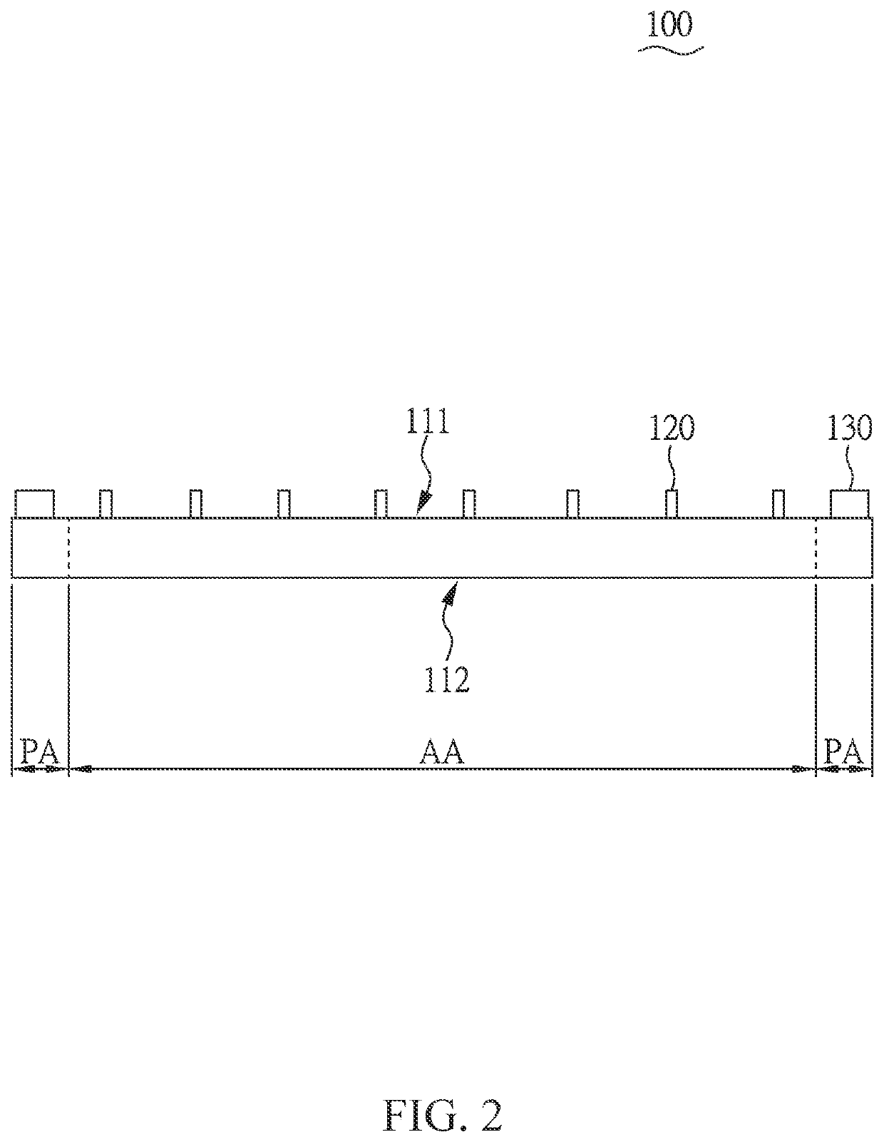
A transparent conductive film and method for making transparent conductive film and touch panel are disclosed. The transparent conductive film includes a substrate and a conductive mesh film. The substrate has a first surface. The conductive mesh film is formed on the first surface of substrate, and the conductive mesh film includes a plurality of silver nanowires. The conductive mesh film includes a plurality of meshes, and the meshes comprise a plurality of traces and a plurality of blank areas. The sheet resistance of the conductive mesh film is 5 Ω / sq to 30 Ω / sq, the width of each of the traces is 1 μm to 10 μm, and a transparency of the conductive mesh film to visible light is greater than 85%.

Description

BACKGROUND OF THE DISCLOSURE1. Field of the Disclosure[0001]The present disclosure relates to a transparent conductive film. More particularly, the present disclosure relates to a transparent conductive film and a manufacturing method of the transparent conductive film for manufacturing a touch panel.2. Description of Related Art[0002]Recently, the application of touch panels is becoming more extensive. More and more electronic products are equipped with touch panels to provide the functions of direct operation or issuing commands for making those electronic products user-friendly. In the current manufacturing process of touch panels, the metal mesh is made of thin-film metal to achieve good penetration. However, the metal mesh made of thin-film metal has poor flexibility and is easily broken due to bending. Moreover, in general, the metal mesh made of thin-film metal requires additional metal wires to connect with the lines in the peripheral area, and the combination of the metal m...

Claims


Application Information

Patent Timeline
IPC IPC(8): G06F3/044G06F3/041
CPCG06F3/044G06F3/0412G06F2203/04103G06F2203/04112
Inventor HSIAO, CHUNG-CHINLIEN, SIOU-CHENGCHIU, YI-WENTSAI, CHIA-YANG
Owner CAMBRIOS FILM SOLUTIONS CORP
Learn More