Thin-film transistor array, image display device, and method for manufacturing thin-film transistor array
- Summary
- Abstract
- Description
- Claims
- Application Information
AI Technical Summary
Benefits of technology
Problems solved by technology
Method used
Image
Examples
first embodiment
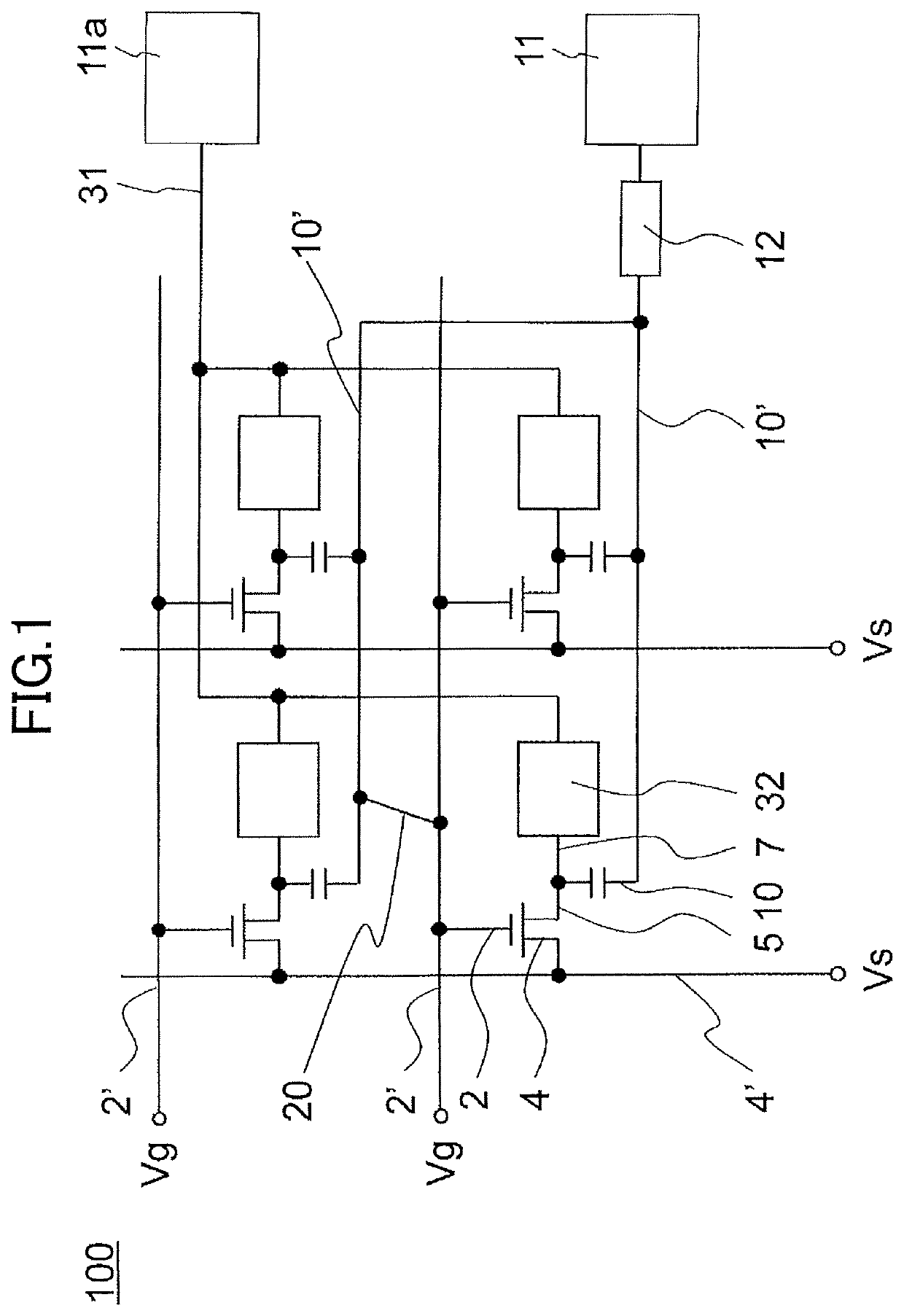
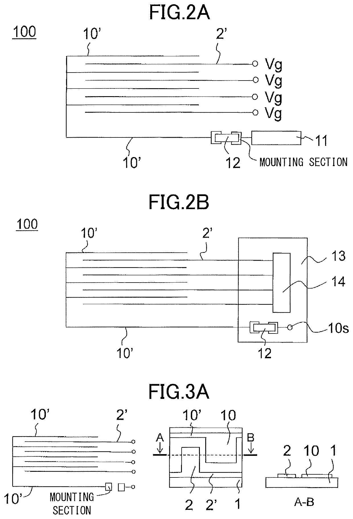
[0038]FIG. 1 illustrates a thin-film transistor array 100 of a first embodiment. The thin-film transistor array 100 includes: an insulating substrate 1; a plurality of gate electrodes 2, a plurality of gate wires 2′ connected to the gate electrodes 2, and a plurality of capacitor electrodes 10, and a plurality of capacitor wires 10′ connected to the capacitor electrodes 10, which are all formed on top of the insulating substrate 1; a gate insulating film 3 which is formed on top of the insulating substrate 1, the gate electrodes 2, the gate wires 2′, the capacitor electrodes 10 and the capacitor electrodes 10; and a plurality of source electrodes 4, a plurality of source wires 4′ connected to the source electrodes 4, a plurality of drain electrodes 5, and a plurality of pixel electrodes 7 connected to the drain electrodes 5, which are all formed on top of the gate insulating film 3. In the thin-film transistor array 100: the pixel electrodes 7 are laid over the respective capacitor ...
second embodiment
[0053]FIG. 4 illustrates a thin-film transistor array 200 of a second embodiment. The thin-film transistor array 200 includes: an insulating substrate 1; a plurality of gate electrodes 2, a plurality of gate wires 2′ connected to the gate electrodes 2, a plurality of capacitor electrodes 10, a plurality of capacitor wires 10′ connected to the capacitor electrodes 10, which are all formed on top of the insulating substrate 1; a gate insulating film 3 which is formed on top of the insulating substrate 1, the gate electrodes 2, the gate wires 2′, the capacitor electrodes 10 and the capacitor electrodes 10; a plurality of source electrodes 4, a plurality of source wires 4′ connected to the source electrodes 4, a plurality of drain electrodes 5, and a plurality of pixel electrodes 7 connected to the drain electrodes 5, which are all formed on top of the gate insulating film 3. In the thin-film transistor array 200: the pixel electrodes 7 are laid over the respective capacitor electrodes ...
example 1
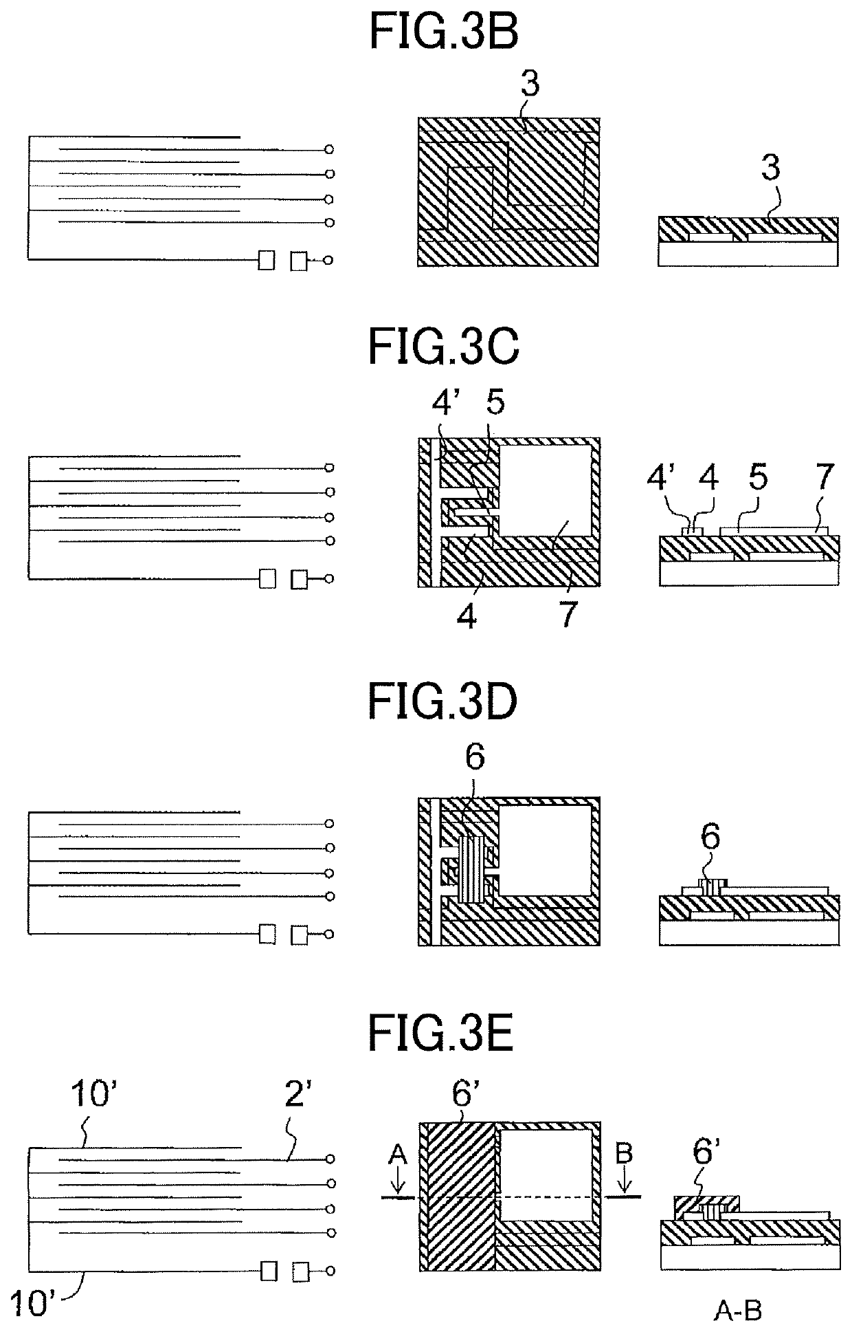
[0078]A specific example will be described. As Example 1, the thin-film transistor array 100 illustrated in FIG. 2A was prepared through the steps illustrated in FIGS. 3A to. 3G. First, using a glass substrate as the insulating substrate 1, Ag ink was off-set printed thereto, followed by baking, thereby forming the gate electrodes 2, the gate wires 2′, the capacitor electrodes 10, and the capacitor wires 10′ (FIG. 3A).
[0079]Then, a polyvinylphenol solution was applied to the resultant object by die coating, followed by baking, thereby forming the gate insulating film 3 (FIG. 3B).
[0080]Then, Ag ink was offset-printed to the resultant object, followed by baking, thereby forming the source electrodes 4, the source wires 4′, the drain electrodes 5, and the pixel electrodes 7 (FIG. 3C). Then, a polythiophene type organic semiconductor solution was printed to the resultant object by flexographic printing, followed by baking, thereby forming the semiconductor layer 6 (FIG. 3D). Then, a flu...
PUM
| Property | Measurement | Unit |
|---|---|---|
| frame time | aaaaa | aaaaa |
| gate voltage | aaaaa | aaaaa |
| gate voltage | aaaaa | aaaaa |
Abstract
Description
Claims
Application Information
 - R&D
- Intellectual Property
- Life Sciences
- Materials
- Tech Scout
- Unparalleled Data Quality
- Higher Quality Content
- 60% Fewer Hallucinations
Browse by: Latest US Patents, China's latest patents, Technical Efficacy Thesaurus, Application Domain, Technology Topic, Popular Technical Reports.
© 2025 PatSnap. All rights reserved.Legal|Privacy policy|Modern Slavery Act Transparency Statement|Sitemap|About US| Contact US: help@patsnap.com


