
Semiconductor device with multiple independent gates

a technology of semiconductor devices and gates, applied in the direction of diodes, electronic switching, pulse techniques, etc., can solve the problems of high voltage and current stress simultaneously, continuous stress on the power device, catastrophic failure, etc., and achieve the effect of facilitating over-voltage protection

Active Publication Date: 2022-01-04
SILICONIX
View PDF187 Cites 1 Cited by
  • Summary
  • Abstract
  • Description
  • Claims
  • Application Information

AI Technical Summary

Benefits of technology

This patent text discusses the need for semiconductor devices with multiple independent gates that have the ability to protect against over-voltage. These systems and methods can be used in both MOSFETs and HEMTs, and are compatible with existing systems and methods in the integrated circuit design process. The technical effect of this patent is the introduction of new semiconductor devices that provide multiple independent gates with over-voltage protection capabilities.

Problems solved by technology

The semiconductor switch needs to absorb this energy stored in the inductive load, which results in high voltage and current stresses simultaneously.
In many applications, particularly in the automotive environments, this situation can happen repeatedly, thereby continuously stressing the power device.
In some cases, the full buildup of this induced potential may far exceed the rated breakdown (V(BR)DSS) of the transistor, thus resulting in catastrophic failure.
Wide bandgap material based switching elements like gallium nitride (GaN) do not have intrinsic body diodes, and as a result have no avalanche capability of any kind.
Their drain source voltage can increase much beyond the rated voltage and, if the unclamped energy is high enough will reach destructive levels.
A single unclamped energy dump can destroy the device completely.

Method used


Image

  • Semiconductor device with multiple independent gates
  • Semiconductor device with multiple independent gates
  • Semiconductor device with multiple independent gates

Examples


Embodiment Construction

[0020]Reference will now be made in detail to various embodiments of the invention, examples of which are illustrated in the accompanying drawings. While the invention will be described in conjunction with these embodiments, it is understood that they are not intended to limit the invention to these embodiments. On the contrary, the invention is intended to cover alternatives, modifications and equivalents, which may be included within the spirit and scope of the invention as defined by the appended claims. Furthermore, in the following detailed description of the invention, numerous specific details are set forth in order to provide a thorough understanding of the invention. However, it will be recognized by one of ordinary skill in the art that the invention may be practiced without these specific details. In other instances, well known methods, procedures, components, and circuits have not been described in detail as not to unnecessarily obscure aspects of the invention.

[0021]Som...


PUM

PropertyMeasurementUnit
structureaaaaaaaaaa
resistanceaaaaaaaaaa
threshold voltageaaaaaaaaaa

Abstract

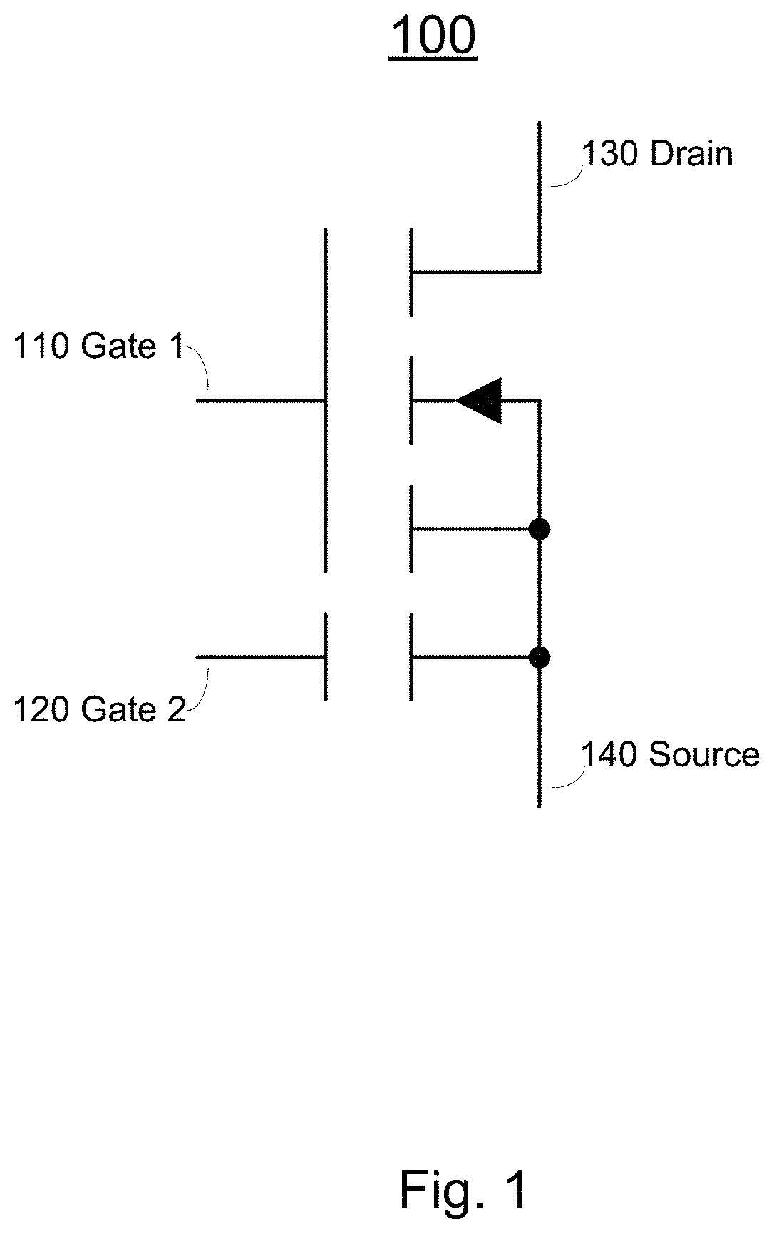
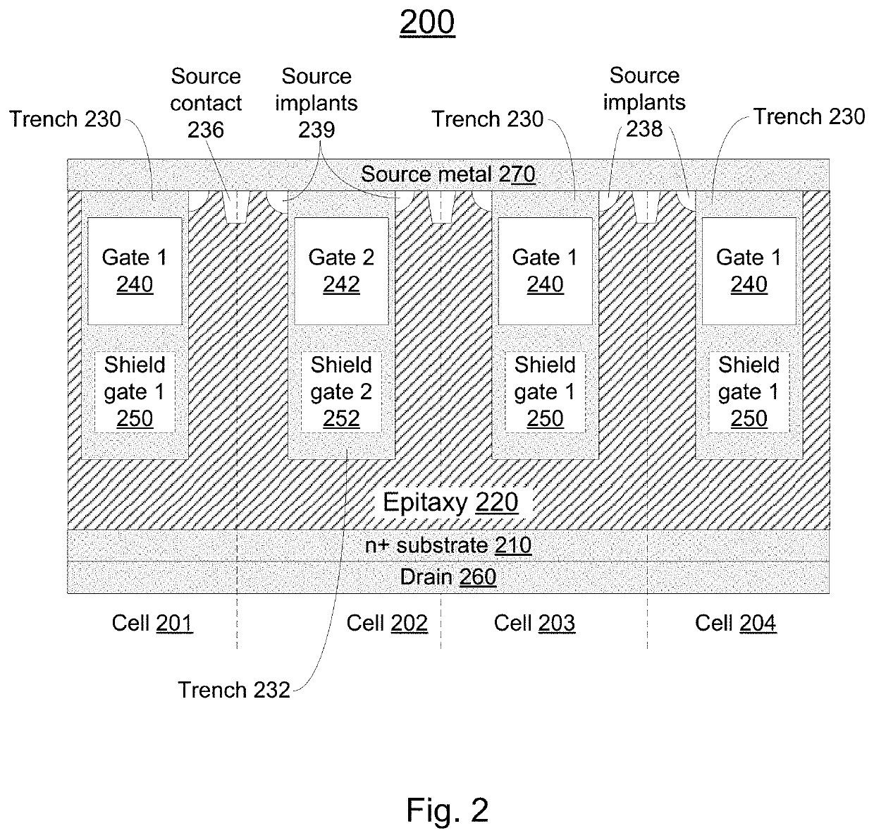
Semiconductor device with multiple independent gates. A gate-controlled semiconductor device includes a first plurality of cells of the semiconductor device configured to be controlled by a primary gate, and a second plurality of cells of the semiconductor device configured to be controlled by an auxiliary gate. The primary gate is electrically isolated from the auxiliary gate, and sources and drains of the semiconductor device are electrically coupled in parallel. The first and second pluralities of cells may be substantially identical in structure.

Description

FIELD OF INVENTION[0001]Embodiments of the present invention relate to the field of integrated circuit design, manufacture, and use. More specifically, embodiments of the present invention relate to systems and methods for semiconductor devices with multiple independent gates.BACKGROUND[0002]Power semiconductors are extensively used in electronic circuits, e.g., power supplies, for switching purposes. System designers using power semiconductors in a wide variety of applications face several challenges to ensure safe and reliable operation under a range of conditions. One extreme condition is Unclamped Inductive Switching (UIS).[0003]Whenever current through an inductive load is quickly turned off, the stored magnetic energy induces a counter electromagnetic force (EMF) that can build up very high potentials across the switch. At the instant of turn off t1, the inductive load L is carrying a peak current of IDSPK. This corresponds to a stored energy of ½L×IDSPK2. The semiconductor sw...

Claims


Application Information

Patent Timeline
Patent Type & Authority Patents(United States)
IPC IPC(8): H03K17/0812H03K17/567H01L27/07H01L29/423H01L29/778H01L29/866H01L29/78H01L29/20
CPCH03K17/08122H01L27/0727H01L29/2003H01L29/4236H01L29/7787H01L29/7808H01L29/7813H01L29/866H03K17/567H01L21/8252H01L27/0605H01L27/0629H01L27/085H01L29/402H01L29/407H01L29/41766H01L29/7786H01L29/7828H03K17/0822H03K2017/6878H03K17/122H01L29/7827
Inventor HAVANUR, SANJAYSHIBIB, M. AYMAN
Owner SILICONIX
Learn More